


Page 1140 - Basic Electrical Engineering
P. 1140
NAND gates. We have known that NOT gates can be built using transistors
               and AND gates can be built using diodes or transistors. The logic circuit in
               which a NOT gate follows an AND gate is called a NOT AND or NAND

               gate. NAND gates can be made with diode–transistors logic (DTL) or
               transistor–transistor logic (TTL).

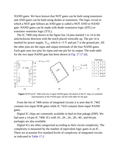
                  The IC 7400 chip shown in the figure has 14 pins marked 1 to 14 in the
               anticlockwise direction with the notch placed vertically up. The pin 14 is

               marked for power supply, V  which is +5 V and pin 7 is the ground pin. All
                                                 CC
               the other pins are the input and output terminals of the four NAND gates.

               Each gate uses two pins for input and one pin for its output. The truth table
               for the two input NAND gate has been shown in Fig. 17.17 (d).


                    Figure 17.17 (a) IC 7400 with four 2-input NAND gates; (b) sketch of the IC chip; (c) symbolic
                                 representation of the NAND gate; (d) the truth table for the gate

                  From the list of 7400 series of integrated circuits it is seen that IC 7402

               contains two-input NOR gates while IC 7410 contains three-input NAND
               gates.
                  Digital IC chips are commonly available in dual-in-line pakage (DIP). We

               had seen a 14-pin IC 7400. ICs with 16-, 20-, 24-, 28-, 40-, and 64-pin
               packages are also available.

                  Digital ICs are often categorized according to their circuit complexity. The
               complexity is measured by the number of equivalent logic gates in an IC.

               There are at present five standard levels of complexity of integrated circuits
               as indicated in Table 17.2.

