
Page 210 - Fiber Optic Communications Fund
P. 210
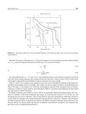
Optical Receivers                                                                  191


                                                  Photon energy (eV)
                                           3   2              1           0.7
                                  10 6


                                                    Ge
                                  10 5                    In 0.7 Ga 0.3 As 0.64 P 0.36
                                 Absorption coefficient (cm −1 )  10 4 3  Si  GaAs
                                                                  In 0.53 Ga 0.47 As


                                                          InP
                                  10


                                  10 2       a–Si:H


                                   10
                                     0.2      0.6       1.0      1.4      1.8
                                                   Wavelength (μm)

           Figure 5.3 Absorption coefficient  versus wavelength (bottom x-axis) or photon energy (top x-axis) for seven common
           semiconductors.


            Therefore, the energy of the photon (∝ f) will not be adequate to excite an electron into the conduction band
           if > , and such a photon will not be absorbed. Eq. (5.2) may be rewritten as
                 co
                                                       hc
                                                   co  =                                   (5.3)
                                                       E g
           or
                                                     1.2
                                               co  =   (μm).                               (5.4)
                                                   E (eV)
                                                    g
            In a silicon photodiode,   ≃ 1.1 μm, so at 1.1 μm, the photon energy is just sufficient to transfer an electron
                                co
           across the silicon energy band gap, thus creating an electron–hole pair, as shown in Fig. 5.4 [5]. As this cutoff
           wavelength is approached, the probability of photon absorption decreases rapidly.
            Table 5.1 shows some common semiconductors used as the active (absorption) materials in photodetectors
           and their corresponding cutoff wavelengths. This results in a spectral range of response of the photodetector,
           that is, the range of wavelengths over which the semiconductor material of the absorption layer of the pho-
           todetector is sensitive to input radiation. Also indicated in Table 5.1 are which semiconductors are direct band
           gap and which are indirect band gap.
            In indirect band-gap semiconductors such as silicon or germanium, photon absorption requires the assis-
           tance of a phonon so that both momentum and energy are conserved (see Section 3.7.3). In this case, the
           absorption process can be sequential, with excited electron–hole pairs thermalizing within their respective
           energy bands by releasing some energy/momentum through phonons. Therefore, compared with absorption
           in a direct band gap where no phonons are involved, absorption in indirect band-gap semiconductors is less
           efficient. Below, we discuss briefly the features of different semiconductor absorption layer materials that
           have been used in commercial photodetectors.