
Page 214 - Fiber Optic Communications Fund
P. 214
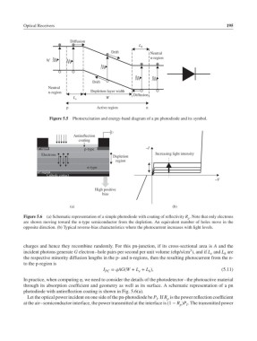
Optical Receivers                                                                  195


                              Diffusion
                                                          L h
                                               Drift           Neutral
                                                               n-region
                    hf


                                       Drift
                     Neutral
                     n-region         Depletion layer width
                                                        Diffusion
                               L e          W
                            p            Active region       n

                     Figure 5.5 Photoexcitation and energy-band diagram of a pn photodiode and its symbol.


                               Antireflection
                                 coating

                p +  region         p-type                   ‒I
                  Electrons                    Depletion         Increasing light intensity
                                                region
                                     n-type
                n +  region
                    Cathode contact
                                                                                         ‒V
                                        High positive
                                           bias

                              (a)                                       (b)

           Figure 5.6  (a) Schematic representation of a simple photodiode with coating of reflectivity R . Note that only electrons
                                                                              p
           are shown moving toward the n-type semiconductor from the depletion. An equivalent number of holes move in the
           opposite direction. (b) Typical reverse-bias characteristics where the photocurrent increases with light levels.


           charges and hence they recombine randomly. For this pn-junction, if its cross-sectional area is A and the
                                                                               3
           incident photons generate G electron–hole pairs per second per unit volume (ehp/s/cm ), and if L and L are
                                                                                       e
                                                                                             h
           the respective minority diffusion lengths in the p- and n-regions, then the resulting photocurrent from the n-
           to the p-region is
                                           I PC  = qAG(W + L + L ),                         (5.11)
                                                              h
                                                          e
           In practice, when computing , we need to consider the details of the photodetector–the photoactive material
           through its absorption coefficient and geometry as well as its surface. A schematic representation of a pn
           photodiode with antireflection coating is shown in Fig. 5.6(a).
            Let the optical power incident on one side of the pn-photodiode be P .If R is the power reflection coefficient
                                                                 I
                                                                      p
           at the air–semiconductor interface, the power transmitted at the interface is (1 − R )P . The transmitted power
                                                                           p
                                                                             I