
Page 2 - 8237A (1)
P. 2
8237A
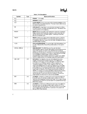
Table 1. Pin Description
Symbol Type Name and Function
V CC POWER: a 5V supply.
V SS GROUND: Ground.
CLK I CLOCK INPUT: Clock Input controls the internal operations of the
8237A and its rate of data transfers. The input may be driven at up
to 5 MHz for the 8237A-5.
CS I CHIP SELECT: Chip Select is an active low input used to select
the 8237A as an I/O device during the Idle cycle. This allows CPU
communication on the data bus.
RESET I RESET: Reset is an active high input which clears the Command,
Status, Request and Temporary registers. It also clears the first/
last flip/flop and sets the Mask register. Following a Reset the
device is in the Idle cycle.
READY I READY: Ready is an input used to extend the memory read and
write pulses from the 8237A to accommodate slow memories or
I/O peripheral devices. Ready must not make transitions during its
specified setup/hold time.
HLDA I HOLD ACKNOWLEDGE: The active high Hold Acknowledge from
the CPU indicates that it has relinquished control of the system
busses.
DREQ0–DREQ3 I DMA REQUEST: The DMA Request lines are individual
asynchronous channel request inputs used by peripheral circuits to
obtain DMA service. In fixed Priority, DREQ0 has the highest
priority and DREQ3 has the lowest priority. A request is generated
by activating the DREQ line of a channel. DACK will acknowledge
the recognition of DREQ signal. Polarity of DREQ is
programmable. Reset initializes these lines to active high. DREQ
must be maintained until the corresponding DACK goes active.
DB0–DB7 I/O DATA BUS: The Data Bus lines are bidirectional three-state
signals connected to the system data bus. The outputs are
enabled in the Program condition during the I/O Read to output
the contents of an Address register, a Status register, the
Temporary register or a Word Count register to the CPU. The
outputs are disabled and the inputs are read during an I/O Write
cycle when the CPU is programming the 8237A control registers.
During DMA cycles the most significant 8 bits of the address are
output onto the data bus to be strobed into an external latch by
ADSTB. In memory-to-memory operations, data from the memory
comes into the 8237A on the data bus during the read-from-
memory transfer. In the write-to-memory transfer, the data bus
outputs place the data into the new memory location.
IOR I/O I/O READ: I/O Read is a bidirectional active low three-state line.
In the Idle cycle, it is an input control signal used by the CPU to
read the control registers. In the Active cycle, it is an output control
signal used by the 8237A to access data from a peripheral during a
DMA Write transfer.
IOW I/O I/O WRITE: I/O Write is a bidirectional active low three-state line.
In the Idle cycle, it is an input control signal used by the CPU to
load information into the 8237A. In the Active cycle, it is an output
control signal used by the 8237A to load data to the peripheral
during a DMA Read transfer.
2