
Page 3 - 8237A (1)
P. 3
8237A
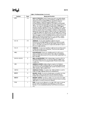
Table 1. Pin Description (Continued)
Symbol Type Name and Function
EOP I/O END OF PROCESS: End of Process is an active low bidirectional
signal. Information concerning the completion of DMA services is
available at the bidirectional EOP pin. The 8237A allows an
external signal to terminate an active DMA service. This is
accomplished by pulling the EOP input low with an external EOP
signal. The 8237A also generates a pulse when the terminal count
(TC) for any channel is reached. This generates an EOP signal
which is output through the EOP line. The reception of EOP, either
internal or external, will cause the 8237A to terminate the service,
reset the request, and, if Autoinitialize is enabled, to write the base
registers to the current registers of that channel. The mask bit and
TC bit in the status word will be set for the currently active channel
by EOP unless the channel is programmed for Autoinitialize. In that
case, the mask bit remains unchanged. During memory-to-memory
transfers, EOP will be output when the TC for channel 1 occurs.
EOP should be tied high with a pull-up resistor if it is not used to
prevent erroneous end of process inputs.
A0–A3 I/O ADDRESS: The four least significant address lines are
bidirectional three-state signals. In the Idle cycle they are inputs
and are used by the CPU to address the register to be loaded or
read. In the Active cycle they are outputs and provide the lower 4
bits of the output address.
A4–A7 O ADDRESS: The four most significant address lines are three-state
outputs and provide 4 bits of address. These lines are enabled
only during the DMA service.
HRQ O HOLD REQUEST: This is the Hold Request to the CPU and is
used to request control of the system bus. If the corresponding
mask bit is clear, the presence of any valid DREQ causes 8237A to
issue the HRQ.
DACK0–DACK3 O DMA ACKNOWLEDGE: DMA Acknowledge is used to notify the
individual peripherals when one has been granted a DMA cycle.
The sense of these lines is programmable. Reset initializes them
to active low.
AEN O ADDRESS ENABLE: Address Enable enables the 8-bit latch
containing the upper 8 address bits onto the system address bus.
AEN can also be used to disable other system bus drivers during
DMA transfers. AEN is active HIGH.
ADSTB O ADDRESS STROBE: The active high, Address Strobe is used to
strobe the upper address byte into an external latch.
MEMR O MEMORY READ: The Memory Read signal is an active low three-
state output used to access data from the selected memory
location during a DMA Read or a memory-to-memory transfer.
MEMW O MEMORY WRITE: The Memory Write is an active low three-state
output used to write data to the selected memory location during a
DMA Write or a memory-to-memory transfer.
PIN5 I PIN5: This pin should always be at a logic HIGH level. An internal
pull-up resistor will establish a logic high when the pin is left
floating. It is recommended however, that PIN5 be connected to
V CC .
3