Page 4 - 8237A (1)
P. 4
8237A


                   FUNCTIONAL DESCRIPTION                  valid DMA requests pending. While in SI, the DMA
                                                           controller is inactive but may be in the Program Con-
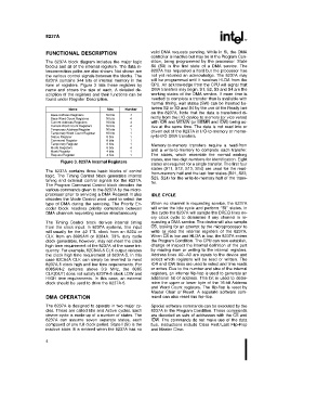
                   The 8237A block diagram includes the major logic  dition, being programmed by the processor. State
                   blocks and all of the internal registers. The data in-  S0 (S0) is the first state of a DMA service. The
                   terconnection paths are also shown. Not shown are  8237A has requested a hold but the processor has
                   the various control signals between the blocks. The  not yet returned an acknowledge. The 8237A may
                   8237A contains 344 bits of internal memory in the  still be programmed until it receives HLDA from the
                   form of registers. Figure 3 lists these registers by  CPU. An acknowledge from the CPU will signal that
                   name and shows the size of each. A detailed de-  DMA transfers may begin. S1, S2, S3 and S4 are the
                   scription of the registers and their functions can be  working states of the DMA service. If more time is
                   found under Register Description.       needed to complete a transfer than is available with
                                                           normal timing, wait states (SW) can be inserted be-
                                                           tween S2 or S3 and S4 by the use of the Ready line
                            Name          Size   Number
                                                           on the 8237A. Note that the data is transferred di-
                     Base Address Registers  16 bits  4
                     Base Word Count Registers  16 bits  4  rectly from the I/O device to memory (or vice versa)
                     Current Address Registers  16 bits  4  with IOR and MEMW (or MEMR and IOW) being ac-
                     Current Word Count Registers  16 bits  4  tive at the same time. The data is not read into or
                     Temporary Address Register  16 bits  1  driven out of the 8237A in I/O-to-memory or memo-
                     Temporary Word Count Register  16 bits  1
                     Status Register      8 bits   1       ry-to-I/O DMA transfers.
                     Command Register     8 bits   1
                     Temporary Register   8 bits   1       Memory-to-memory transfers require a read-from
                     Mode Registers       6 bits   4
                     Mask Register        4 bits   1       and a write-to-memory to complete each transfer.
                     Request Register     4 bits   1       The states, which resemble the normal working
                                                           states, use two digit numbers for identification. Eight
                        Figure 3. 8237A Internal Registers
                                                           states are required for a single transfer. The first four
                                                           states (S11, S12, S13, S14) are used for the read-
                   The 8237A contains three basic blocks of control  from-memory half and the last four states (S21, S22,
                   logic. The Timing Control block generates internal
                   timing and external control signals for the 8237A.  S23, S24) for the write-to-memory half of the trans-
                   The Program Command Control block decodes the  fer.
                   various commands given to the 8237A by the micro-
                   processor prior to servicing a DMA Request. It also  IDLE CYCLE
                   decodes the Mode Control word used to select the
                   type of DMA during the servicing. The Priority En-  When no channel is requesting service, the 8237A
                   coder block resolves priority contention between  will enter the Idle cycle and perform ‘‘SI’’ states. In
                   DMA channels requesting service simultaneously.  this cycle the 8237A will sample the DREQ lines ev-
                                                           ery clock cycle to determine if any channel is re-
                   The Timing Control block derives internal timing  questing a DMA service. The device will also sample
                   from the clock input. In 8237A systems, this input  CS, looking for an attempt by the microprocessor to
                   will usually be the w2 TTL clock from an 8224 or  write or read the internal registers of the 8237A.
                   CLK from an 8085AH or 8284A. 33% duty cycle  When CS is low and HLDA is low, the 8237A enters
                   clock generators, however, may not meet the clock  the Program Condition. The CPU can now establish,
                   high time requirement of the 8237A of the same fre-  change or inspect the internal definition of the part
                   quency. For example, 82C84A-5 CLK output violates  by reading from or writing to the internal registers.
                   the clock high time requirement of 8237A-5. In this  Address lines A0–A3 are inputs to the device and
                   case 82C84A CLK can simply be inverted to meet  select which registers will be read or written. The
                   8237A-5 clock high and low time requirements. For  IOR and IOW lines are used to select and time reads
                   8085AH-2 systems above 3.9 MHz, the 8085  or writes. Due to the number and size of the internal
                   CLK(OUT) does not satisfy 8237A-5 clock LOW and  registers, an internal flip-flop is used to generate an
                   HIGH time requirements. In this case, an external  additional bit of address. This bit is used to deter-
                   clock should be used to drive the 8237A-5.  mine the upper or lower byte of the 16-bit Address
                                                           and Word Count registers. The flip-flop is reset by
                                                           Master Clear or Reset. A separate software com-
                   DMA OPERATION                           mand can also reset this flip-flop.
                   The 8237A is designed to operate in two major cy-  Special software commands can be executed by the
                   cles. These are called Idle and Active cycles. Each  8237A in the Program Condition. These commands
                   device cycle is made up of a number of states. The  are decoded as sets of addresses with the CS and
                   8237A can assume seven separate states, each  IOW. The commands do not make use of the data
                   composed of one full clock period. State I (SI) is the  bus. Instructions include Clear First/Last Flip-Flop
                   inactive state. It is entered when the 8237A has no  and Master Clear.

                   4

