
Page 350 - Maxwell House
P. 350
330 Chapter 6
possible radiation loss but keep the top
E-field grounding side strips and bottom
grounding plane electrically
equipotential. Consequently, the
existence of the whole set of high
modes in such multi-wire system (part
of them are also quasi TEM-modes)
becomes almost impossible that
stabilizes the dominant mode
H-field
propagation. That allows using GCPW
at much higher frequencies (up to 30
GHz and higher) than microstrip as the
high mode propagation is an issue.
c) 7. The same way as microstrip
and slotline, CPW and GCPW feature
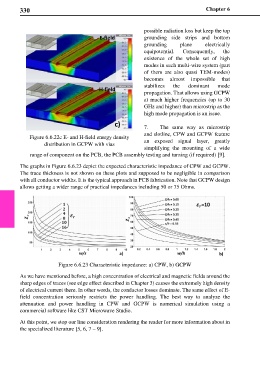
Figure 6.6.22c E- and H-field energy density
distribution in GCPW with vias an exposed signal layer, greatly
simplifying the mounting of a wide
range of component on the PCB, the PCB assembly testing and turning (if required) [9].
The graphs in Figure 6.6.23 depict the expected characteristic impedance of CPW and GCPW.
The trace thickness is not shown on these plots and supposed to be negligible in comparison
with all conductor widths. It is the typical approach in PCB fabrication. Note that GCPW design
allows getting a wider range of practical impedances including 50 or 75 Ohms.
Figure 6.6.23 Characteristic impedance: a) CPW, b) GCPW
As we have mentioned before, a high concentration of electrical and magnetic fields around the
sharp edges of traces (see edge effect described in Chapter 3) causes the extremely high density
of electrical current there. In other words, the conductor losses dominate. The same effect of E-
field concentration seriously restricts the power handling. The best way to analyze the
attenuation and power handling in CPW and GCPW is numerical simulation using a
commercial software like CST Microwave Studio.
At this point, we stop our line consideration rendering the reader for more information about in
the specialized literature [5, 6, 7 – 9].