
Page 345 - Maxwell House
P. 345
FEED LINE BASICS 325
2. E-field vector lines are perpendicular while H-field vector lines are tangential to the metal
elements of the stripline. The lion’s share of electric and magnetic energy is concentrated
in the gaps between the strip and ground plane as long as ℎ ≪ and ≪ . The peripheral
fields outside the strip carry small energy and decay exponentially (all fields are in dB-
scale) as the distance from the strip edges increases. If so, the crosstalk is relatively low
(but higher than in a symmetrical stripline) meaning that the microstrip supports densely
integrated circuits and is well suited for fabricating multilayer circuits.
3. The edge effect discussed in Chapter 3 is clearly visible. According to Table 3.1 of this
⁄
chapter, the radial field variation around the vertexes are −1 3 . Apparently, these vertexes
must be rounded at higher level of transmitting power.
4. The second ground plane above the strip or full shielding housing like a metal box with
germetization practically always in use to prevent the environmental impact and suppress
possible EM interferences.
5. Following the same path as in a stripline, we obtain from (6.9) = ∫ ∘ = ℎ
and = ∮ ∘ = ( + 2). The integration path for the current is almost two time
shorter than in the case of a stripline because the magnetic field intensity is minor in area
above the strip. Therefore,
ℎ 1
= ⁄ ~ = (6.43)
⁄
⁄
+2 ℎ+2 ℎ
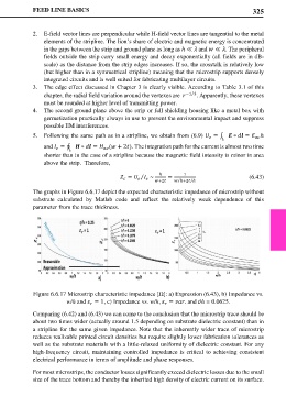
The graphs in Figure 6.6.17 depict the expected characteristic impedance of microstrip without
substrate calculated by Matlab code and reflect the relatively weak dependence of this
parameter from the trace thickness.
Figure 6.6.17 Microstrip characteristic impedance [Ω]: a) Expression (6.43), b) Impedance vs.
w/h and = 1, c) Impedance vs. w/h, = . and t/h = 0.0625.
Comparing (6.42) and (6.43) we can come to the conclusion that the microstrip trace should be
about two times wider (actually around 1.5 depending on substrate dielectric constant) than in
a stripline for the same given impedance. Note that the inherently wider trace of microstrip
reduces realizable printed circuit densities but require slightly lower fabrication tolerances as
well as the substrate materials with a little-relaxed uniformity of dielectric constant. For any
high-frequency circuit, maintaining controlled impedance is critical to achieving consistent
electrical performance in terms of amplitude and phase responses.
For most microstrips, the conductor losses significantly exceed dielectric losses due to the small
size of the trace bottom and thereby the inherited high density of electric current on its surface.