
Page 344 - Maxwell House
P. 344
324 Chapter 6
and field symmetry is shown in Figure 6.6.13. Evidently, the circuit elements like lumped or
distributed inductors, capacitors, semiconductors, etc. adjacent or connected to strip should not
disturb this symmetry. The Ohmic loss is proportional to the density of electric current on metal
line elements. Evidently, this density is higher on the surface of strip making it the largest source
of conductive loss. The latter may exceed the dielectric loss and dominate at frequencies above
10 GHz while → 0 to prevent the high mode propagation. According to the first equation in
(3.52) from Chapter 3 the dielectric loss is proportional to the frequency and loss tangent of
dielectric filling. The best and accurate way to calculate all kind of loss is numerical simulation.
The stripline peak power handling is limited by the breakdown between the strip and ground
planes. The complexity of the EM field structure and edge effect impede the peak power
analysis and make it almost impossible without numerical simulation. The particular attention
should be devoted to elements providing the transition from stripline to the coaxial line or any
other type of feed line. The same holds for the estimation of average power handling restricted
mainly by the maximum allowable temperature of the dielectric.
6.6.7 Microstrip
As we have mentioned before, this line relates to the class of planar open lines supporting DC
power transfer. As such, the frequency independent dominant mode is the TEM in lines without
dielectric layer and quasi-TEM (hybrid to be exact) if the substrate supports the strip. Microstrip
circuits are easier (and less expensive) to fabricate than stripline, with less processing steps and
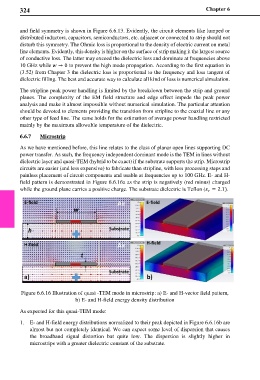
painless placement of circuit components and usable at frequencies up to 100 GHz. E- and H-
field pattern is demonstrated in Figure 6.6.16a as the strip is negatively (red minus) charged
while the ground plane carries a positive charge. The substrate dielectric is Teflon ( = 2.1).
Figure 6.6.16 Illustration of quasi -TEM mode in microstrip: a) E- and H-vector field pattern,
b) E- and H-field energy density distribution
As expected for this quasi-TEM mode:
1. E- and H-field energy distributions normalized to their peak depicted in Figure 6.6.16b are
almost but not completely identical. We can expect some level of dispersion that causes
the broadband signal distortion but quite low. The dispersion is slightly higher in
microstrips with a greater dielectric constant of the substrate.