
Page 214 - Wago_PCB_TerminalBlocksConnectors_Volume2_2015_US
P. 214
SMD Terminal Blocks with Push-Buttons, 0.75 mm 2
2 Pin Spacing: 8 mm
212 2060 Series
● SMD terminal blocks with CAGE CLAMP S and push-buttons
®
● 8 mm pin spacing version for higher rated voltages
● Push-in termination of solid and ferruled conductors
● Convenient termination/removal of fine-stranded conductors via
push-buttons
● Height of just 4.5 mm minimizes on-board LED shadowing
● Available in tape-and-reel packaging for automated assembly
● For THR version, see page 125.
Technical data:
8 mm
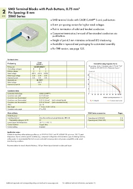
Pin Spacing 0.314 in. Current-Carrying Capacity Curve
2
Ratings per IEC/EN 60664-1 Pin spacing: 4 mm / Conductor size: 0.75 mm “f-st”
Based on: EN 60512-5-2 / Reduction factor: 1
Overvoltage category III III II
Pollution degree 3 2 2 Current in A
Rated voltage 400 V 630 V 1000V
Rated surge voltage 6 kV 6 kV 6 kV 20
Nominal current 9 A 9 A 9 A
Approvals per UL 1977 15
Rated voltage 600 V
Nominal current UL 9 A 10
5
Conductor data:
Connection technology CAGE CLAMP S 0 10 20 30 40 50 60 70 80 90 100105
®
Conductor size: solid 0.2–0.75 mm 2
Conductor size: fine-stranded 0.2–0.75 mm 2 Ambient operating temperature in °C
Conductor size: fine-stranded 0.25–0.34 mm 2 (with insulated ferrule) 2-, 4-, 6-pole Conductor rated current
Conductor size: fine-stranded 0.25–0.34 mm 2 (with uninsulated ferrule)
AWG 24–18
Strip length 7–9 mm / 0.28–0.35 in.
Conductor entry angle 0° to PCB
Material data: 2060 Series accessories: Pages:
Material group I
Insulating material Glass-fiber-reinforced polyphthalamide (PPA-GF) Operating tool (206-860) 218
Flammability rating per UL 94 0V Operating tool (2060-189) 218
Lower/Upper limit temperature -60 °C / +105 °C
Contact material Copper alloy
Contact plating tin-plated
Application notes:
Suitable for lead-free, reflow-soldering profiles acc. to DIN EN 61760-1 and IEC 60068-2-58 up to max. 260 °C peak
temperature. Due to customer specific variables (e.g., component configuration and orientation, type of soldering machine,
solder paste), it is recommended that trial runs are conducted to ensure product and process compatibility under actual
manufacturing conditions.
Recommendation for stencil: Material thickness, 150 µm. Pattern layout identical to solder pad layout.
Additional approvals and corresponding ratings can be found at www.wago.com. For additional technical information, see Section 13.