
Page 276 - Mechatronics with Experiments
P. 276
JWST499-Cetinkunt
JWST499-c05
262 MECHATRONICS Printer: Yet to Come October 28, 2014 11:15 254mm×178mm
14 e –
+
(a) (b)
Si Si Si
Si Si
Si Si Si
Si Si
Si Si Si
(c)
Si Si Si Si Si Si
Si Si Si Si
Si B Si Si P Si
Electron
Si Hole Si Si Si
Si Si Si Si Si Si
(d) p-type semiconductor (e) n-type semiconductor
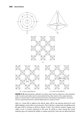
FIGURE 5.10: Semiconductor materials: (a) a silicon atom has four electrons in the outermost
oribit. (b and c) each silicon atom is surrounded by four other atoms in the crystal structure
where it is shown both in three-dimensional and two-dimensional representation. (d) p-type,
and (e) n-type semiconductor material (doped silicon) crystal structure.
table (i.e., boron (B)) is added to the silicon, there will be one missing electron for each
added impurity atom in the crystal structure. One of the four connections around the group
III atom will be missing an electron (Figure 5.10d). This effective positive charge, also
called a hole, is loosely connected to the atom. Its ability to move around the crystal
structure gives the material the ability to conduct electricity. Since the net added electrical