Page 278 - Mechatronics with Experiments
P. 278

JWST499-Cetinkunt
            JWST499-c05
                       264   MECHATRONICS  Printer: Yet to Come                     October 28, 2014 11:15 254mm×178mm
                                                                                  i
                                                                                  D
                                                                     Reverse  Reverse Forward  Forward
                                                           i        breakdown   bias  bias    breakdown
                                                           D
                                                                      region   region  region  region
                                                                          V  Z
                                                    +           _
                                                                                         V    V
                                                          V                               F    D
                                                           D
                                       (a)
                                                                        i                i
                                                                         S
                                                                                          L
                                                                       R      i
                                                                        S      Z
                                            _               V
                                +                            S                             V
                                                                         V                  L
                                      V                                   Z            R
                                       D                                                L
                                       (b)
                                                                               Voltage
                                                                               regulator

                                       A                                    i
                                                                             AK
                                                   A                                     i
                                                                                          G
                                      P                i
                                      n                AK             V RB
                              Gate (G)                 V A
                                      P                                                     V
                                           G           K                               V     AK
                                      n                                                 FB
                                                   K
                                       K
                                      (c)
                                                                             i
                                                                             AK
                                         A
                                                                                              i
                                               i                                              G
                                               AK
                                                                –V FB
                              G                V                                                V
                                               AK                                          V     AK
                                                                                            FB
                                         K
                                      (d)

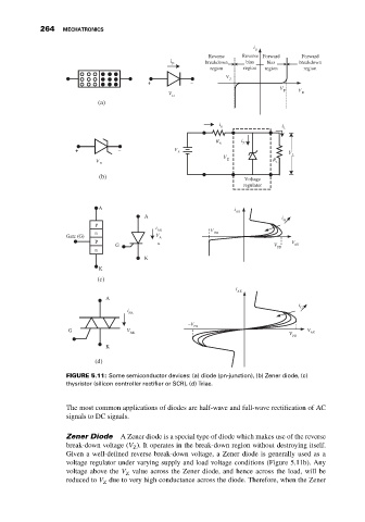
                              FIGURE 5.11: Some semiconductor devices: (a) diode (pn-junction), (b) Zener diode, (c)
                              thysristor (silicon controller rectifier or SCR), (d) Triac.


                              The most common applications of diodes are half-wave and full-wave rectification of AC
                              signals to DC signals.

                              Zener Diode    A Zener diode is a special type of diode which makes use of the reverse
                              break-down voltage (V ). It operates in the break-down region without destroying itself.
                                                Z
                              Given a well-defined reverse break-down voltage, a Zener diode is generally used as a
                              voltage regulator under varying supply and load voltage conditions (Figure 5.11b). Any
                              voltage above the V value across the Zener diode, and hence across the load, will be
                                              Z
                              reduced to V due to very high conductance across the diode. Therefore, when the Zener
                                        Z
   273   274   275   276   277   278   279   280   281   282   283