Page 294 - Mechatronics with Experiments
P. 294

JWST499-Cetinkunt
            JWST499-c05
                       280   MECHATRONICS  Printer: Yet to Come                     October 28, 2014 11:15 254mm×178mm
                                   Notice that as long as the Zener diode is conducting, the voltage across the base and
                              ground will be V = V , and the maximum base current is
                                           B
                                                Z
                                                         i = (V CC1  − V )∕R 1                  (5.170)
                                                          B
                                                                     Z
                              The voltage between the emitter and ground is
                                                       V = V − V BE  = V − 0.7                  (5.171)
                                                        E
                                                                       Z
                                                             Z
                              Hence, current across the resistor R is
                                                          E
                                                      i = V ∕R = (V − 0.7)∕R E                  (5.172)
                                                              E
                                                           E
                                                                    Z
                                                      E
                              The collector current which also is the load current is
                                                                        
                                                        i = i − i =      i E                    (5.173)
                                                             E
                                                         C
                                                                 B
                                                                        + 1
                              Notice that i is very small compared to i .The i is constant as long as the V  > V and
                                        B                     E     E                      CC1   Z
                              the R is constant. Therefore, the i will remain a constant current despite the variations in
                                  E                      C
                              the load resistance R .
                                              L
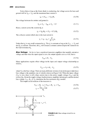
                              Bias Voltage   So far we have considered transistor amplifiers that amplify current or
                              voltage and that when the input signal is zero, the output signal is zero as well, that is
                                                            V out  = K ⋅ V in                   (5.174)
                                                                   v
                              Many applications require offset voltage in the input and output voltage relationship as
                              follows,

                                                          V out  = V + K ⋅ V in                 (5.175)
                                                                     v
                                                                 0
                              where V is the bias voltage. There are many different versions of circuit designs to introduce
                                    0
                              bias voltage to the amplifier, one of which is shown in Figure 5.22. When the input voltage
                              (V ) is zero, there is still a base current due to the power supply voltage (V CC ) and the
                                in
                              resistor R . Given the supply voltage, load resistance, amplifier current gain, and the desired
                                     B
                              bias voltage: V  , R ,   , V , determine the bias resistance (R ) needed.
                                          CC  L    0                          B
                                   The output circuit relation of the transistor is
                                                   V   = R ⋅ i + V  = R ⋅ i + V                 (5.176)
                                                    CC    L  C   CE    L  C    out
                                                         V CC  − V out
                                                    i =                                         (5.177)
                                                     C
                                                            R L
                                                             V
                                                              CC
                                          R         R
                                           B         L
                                                           v out  = V o
                                           i
                                           B
                                                     i c
                                v in


                                                                   FIGURE 5.22: Bias voltage circuit for an
                                                                   amplifier.
   289   290   291   292   293   294   295   296   297   298   299