Page 292 - Mechatronics with Experiments
P. 292

JWST499-Cetinkunt
            JWST499-c05
                       278   MECHATRONICS  Printer: Yet to Come                     October 28, 2014 11:15 254mm×178mm
                              transistor. The diode limits the voltage to the supply voltage by providing a current flow
                              path during that transient period. The current flow due to inductive voltage is then dissipated
                              in the diode-load loop within a short period of time. The resistor (R ) which connects the
                                                                                    2
                              base to the ground is not necessary, but makes the circuit a better one by providing a ground
                              to the base when the transistor is not turned ON (when the mechanical switch is open).
                              In the following discussion, assume the components in the dotted blocks do not exist for
                              simplicity. Let L = 0.0 H and R = 0.0 Ω. When the mechanical switch is OFF, the base
                                                       2
                              voltage and current are zero, the transistor is OFF, no current flows through the load. When
                              the mechanical switch is ON, the base current and collector current are,
                                                        V AB  (10 − 0.7)V
                                                   i =      =           = 9.3 mA                (5.156)
                                                    B
                                                        R       1000 Ω
                                                          1
                                                   i =    ⋅ i = 0.93 A                          (5.157)
                                                    C
                                                           B
                              where it is assumed that    = 100. But the maximum current that the supply can support is
                                                        V CC  − V CE  10 − 0.2
                                                i C,max  =       =         = 0.098 A            (5.158)
                                                           R L       100
                              Hence, the transistor saturates with the maximum voltage drop across the load, V = 10 −
                                                                                              L
                              0.2, and the minimum voltage drop across the transistor, V CE  = 0.2 V. The transistor acts
                              like a very low resistance switch when it is saturated. Voltage drop across it is V CE  = 0.2V.
                              Providing excess base current to saturate the transistor is a good idea and provides a safety
                              margin to make sure the transistor is fully turned ON (in its saturation region) and hence
                              providing the maximum voltage drop across the load. Notice that when the transistor is
                              ON, the current drain through the resistor R is
                                                                 2
                                                         V BE    0.7
                                                     i =     =        = 0.07 mA                 (5.159)
                                                      2
                                                          R 2  10 000
                              which is a negligable load.

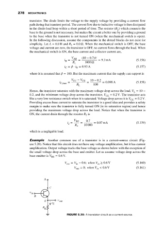
                              Example    Another common use of a transistor is in a current-source circuit (Fig-
                              ure 5.20). Notice that this circuit does not have any voltage amplification, but it has current
                              amplification. Output voltage tracks the base voltage as shown below with the exception of
                              the small voltage drop across the base and emitter. Let us assume voltage drop across the
                              base-emitter is V  = 0.6V.
                                           BE
                                                    V out  = V − 0.6; when V ≥ 0.6 V            (5.160)
                                                                        in
                                                           in
                                                         V out  = 0; when V < 0.6 V             (5.161)
                                                                       in
                                       A

                                          C
                              v in
                                 B
                                       E       v out
                                           i E
                                      R
                                       E
                                                     FIGURE 5.20: A transistor circuit as a current-source.
   287   288   289   290   291   292   293   294   295   296   297