
Page 287 - Mechatronics with Experiments
P. 287
Printer: Yet to Come
October 28, 2014 11:15 254mm×178mm
JWST499-c05
JWST499-Cetinkunt
ELECTRONIC COMPONENTS FOR MECHATRONIC SYSTEMS 273
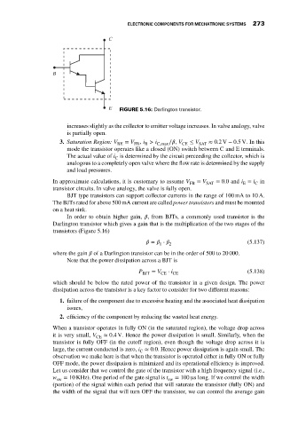
C
B
E FIGURE 5.16: Darlington transistor.
increases slightly as the collector to emitter voltage increases. In valve analogy, valve
is partially open.
3. Saturation Region: V BE = V , i > i C,max ∕ , V CE ≤ V SAT ≈ 0.2V − 0.5V. In this
FB
B
mode the transistor operates like a closed (ON) switch between C and E terminals.
The actual value of i is determined by the circuit preceeding the collector, which is
C
analogous to a completely open valve where the flow rate is determined by the supply
and load pressures.
In approximate calculations, it is customary to assume V FB = V SAT = 0.0 and i = i in
C
E
transistor circuits. In valve analogy, the valve is fully open.
BJT type transistors can support collector currents in the range of 100 mA to 10 A.
The BJTs rated for above 500 mA current are called power transistors and must be mounted
on a heat sink.
In order to obtain higher gain, , from BJTs, a commonly used transistor is the
Darlington transistor which gives a gain that is the multiplication of the two stages of the
transistors (Figure 5.16)
= ⋅ (5.137)
1 2
where the gain of a Darlington transistor can be in the order of 500 to 20 000.
Note that the power dissipation across a BJT is
P BJT = V CE ⋅ i CE (5.138)
which should be below the rated power of the transistor in a given design. The power
dissipation across the transistor is a key factor to consider for two different reasons:
1. failure of the component due to excessive heating and the associated heat dissipation
issues,
2. efficiency of the component by reducing the wasted heat energy.
When a transistor operates in fully ON (in the saturated region), the voltage drop across
it is very small, V ≈ 0.4 V. Hence the power dissipation is small. Similarly, when the
CE
transistor is fully OFF (in the cutoff region), even though the voltage drop across it is
large, the current conducted is zero, i ≈ 0.0. Hence power dissipation is again small. The
C
observation we make here is that when the transistor is operated either in fully ON or fully
OFF mode, the power dissipation is minimized and its operational efficiency is improved.
Let us consider that we control the gate of the transistor with a high frequency signal (i.e.,
w sw = 10 KHz). One period of the gate signal is t sw = 100 μs long. If we control the width
(portion) of the signal within each period that will saturate the transistor (fully ON) and
the width of the signal that will turn OFF the transistor, we can control the average gain