Page 286 - Mechatronics with Experiments
P. 286

JWST499-Cetinkunt
            JWST499-c05
                       272   MECHATRONICS  Printer: Yet to Come                     October 28, 2014 11:15 254mm×178mm
                                   Collector (C)        Collector (C)


                              Base (B)             Base (B)


                                   Emitter (E)           Emitter (E)

                                       n-p-n transistor         p-n-p transistor
                                                         (a)

                                               +                       –
                              Drain                   Drain
                              Gate                    Gate
                                           +     0                 +     0
                                                   –                       +
                              Source                  Source

                               n-channel MOSFET         p-channel MOSFET
                                                         (b)


                                     Schematic symbol     Equivalent circuit
                                                         (c)
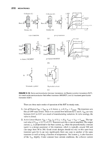
                              FIGURE 5.15: Some semiconductor devices: transistors. (a) Bipolar junction transistors (BJT),
                              (b) metal oxide semiconductor field effect transistor (MOSFET), and (c) insulated gate bipolar
                              transistor (IGBT).


                                   There are three main modes of operation of the BJT in steady-state,

                                1. Cut-off Region:V  < V , i = 0, hence, i = 0, V  > V  . The transistor acts
                                                BE    FB B           C      CE    supply
                                   like an OFF-state switch. There is no current flow between the C and E. V  can vary
                                                                                             FB
                                   between 0.6V to 0.8 V as a result of manufacturing variations. In valve analogy, the
                                   valve is closed.
                                2. Active Linear Region: V  = V , i ≠ 0; i =    i , V  < V  < V  . The typ-
                                                      BE   FB  B     C    B   SAT   CE    supply
                                   ical value of V  ≈ 0.2V to 0.5 V. Transistor acts like a current amplifier. The output
                                              SAT
                                   current, i , is proportional to the base current, i , where the proportionality constant
                                          C
                                                                        B
                                   (gain) is a design parameter of the transistor, which is typically around 100 and
                                   can range from 50 to 200. Good circuit designs should not rely on this open-loop
                                   transistor gain for it can vary significantly from one copy to another of the same
                                   transistor as well as being a function of temperature. The current i is also function
                                                                                        C
                                   of the V CE  slightly. Under constant base current conditions, the collector current
   281   282   283   284   285   286   287   288   289   290   291