
Page 288 - Mechatronics with Experiments
P. 288
JWST499-Cetinkunt
JWST499-c05
274 MECHATRONICS Printer: Yet to Come October 28, 2014 11:15 254mm×178mm
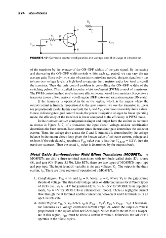
R
2
C i
c
R B
1
V
V i CC2
CC1 B
E
FIGURE 5.17: Common emitter configuration and voltage amplifier usage of a transistor.
of the transistor by the average of the ON–OFF widths of the gate signal. By increasing
and decreasing the ON–OFF width periods within each t sw period, we can vary the net
average gain. Since only two states of transistor control are needed, the gate signal only has
to have two voltage levels: a high level to saturate the transistor and a low level to cutoff
the transistor. Then the only control problem is controlling the ON–OFF widths of the
switching pulses. This is called the pulse width modulated (PWM) control of transistors.
The PWM control method results in more efficient operation of the transistors. It operates a
transistor in one of two regions: cutoff region (OFF state) and saturation region (ON state).
If the transistor is operated in the active region, which is the region where the
output current is linearly proportional to the gate current, we use the transistor in linear
(or proportional) mode. In this case both the i and V CE can have reasonably finite values.
C
Hence, in linear gate signal control mode, the power dissipation is larger. In linear operating
mode, the efficiency of the transistor is lower compared to the efficiency in PWM mode.
In the common-emitter configuration (input and output have the emitter as common
as shown in Figure 5.17) of a transistor, the input circuit voltage–resistor combination
determines the base current. Base current times the transistor gain determines the collector
current. Then, the voltage drop across the C and E terminals is determined by the voltage
balance in the output circuit loop given the known value of collector current, voltage and
resistor. If the calculated i requires a V CE value that is less than V CE,sat = 0.2 V, then the
C
transistor saturates. Then the actual i value is determined by the output circuit.
C
Metal Oxide Semiconductor Field Effect Transistors (MOSFETs) A
MOSFETs are also a three-terminal transistors with terminals called drain (D), source
(S), and gate (G) (Figure 5.13b). Like BJTs, there are two types of MOSFETs: npn-type
and pnp-type. The input (control) variable is the gate voltage, V . The output is the drain
G
current, i . There are three regions of operation of a MOSFET,
D
1. Cutoff Region: V < V and i = 0, hence, i = 0, where V is the gate-source
GS T G D T
threshold voltage. The threshold voltage takes on different values for different types
of FETs (i.e., V ≈−4 V for junction FETs, V ≈−5 V for MOSFETs in depletion
T T
mode, V ≈ 4 V for MOSFETs in enhancement mode). There is negligible current
T
flow through the D terminal and the connection between D and S terminals is in an
open switch state.
2
2. Active Region: V GS > V , hence, i ∝ (V GS − V ) , V DS > (V GS − V ). The transis-
T
T
D
T
tor functions as a voltage controlled current amplifier, where the output current is
proportional to the square of the net GS voltage. Notice that for the MOSFET to oper-
ate in this region, V DS must be above a certain threshold. Otherwise, the MOSFET
operates in the ohmic region.