
Page 318 - Basic Electrical Engineering
P. 318
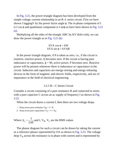
In Fig. 3.21, the power triangle diagram has been developed from the
               simple voltage–current relationship in an R–L series circuit. First we have
               shown I laggingV by the power factor angle ϕ. The in-phase component of I

               is I cos ϕ and quadratuse component is I sinϕ as have been shown in Fig. 3.21
               (a).

                  Multiplying all the sides of the triangle ABC by KV (kilo-volt), we can
               draw the power triangle as in Fig. 3.21 (b)


                                                    kVA cos ϕ = kW
                                                  kVA sin ϕ = kVAR


                  In the power triangle diagram, if θ is taken as zero, i.e., if the circuit is

               resistive, reactive power, Q becomes zero. If the circuit is having pure
               inductance or capacitance, ϕ = 90, active power, P becomes zero. Reactive

               power will be present whenever there is inductance or capacitance in the
               circuit. Inductors and capacitors are energy-storing and energy-releasing

               devices in the form of magnetic and electric fields, respectively, and are of
               importance in the field of electrical engineering.


                                               3.2.5 R—C Series Circuit

               Consider a circuit consisting of a pure resistance R and connected in series

               with a pure capacitor C across an ac supply of frequency f as shown in Fig.
               3.22.

                  When the circuit draws a current I, then there are two voltage drops.

                   i.  Drop across pure resistance V  = I × R
                                                R
                  ii.  Drop across pure capacitance V  = I × X C
                                                  C


               Where                 and I, V , V  are the RMS values
                                                    C
                                               R

                  The phasor diagram for such a circuit can be drawn by taking the current
               as a reference phasor represented by OA as shown in Fig. 3.23. The voltage

               drop V  across the resistance is in phase with current and is represented by
                        R