


Page 956 - Basic Electrical Engineering
P. 956
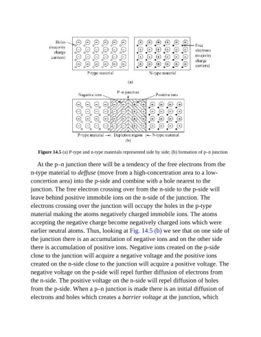
Figure 14.5 (a) P-type and n-type materials represented side by side; (b) formation of p–n junction


                  At the p–n junction there will be a tendency of the free electrons from the
               n-type material to deffuse (move from a high-concertration area to a low-
               concertion area) into the p-side and combine with a hole nearest to the

               junction. The free electron crossing over from the n-side to the p-side will
               leave behind positive immobile ions on the n-side of the junction. The

               electrons crossing over the junction will occupy the holes in the p-type
               material making the atoms negatively charged immobile ions. The atoms

               accepting the negative charge become negatively charged ions which were
               earlier neutral atoms. Thus, looking at Fig. 14.5 (b) we see that on one side of

               the junction there is an accumulation of negative ions and on the other side
               there is accumulation of positive ions. Negative ions created on the p-side
               close to the junction will acquire a negative voltage and the positive ions

               created on the n-side close to the junction will acquire a positive voltage. The
               negative voltage on the p-side will repel further diffusion of electrons from

               the n-side. The positive voltage on the n-side will repel diffusion of holes
               from the p-side. When a p–n junction is made there is an initial diffusion of
               electrons and holes which creates a barrier voltage at the junction, which

