


Page 958 - Basic Electrical Engineering
P. 958
terminal on the p-side, the p–n junction is said to be a reverse-biased
               junction.


               (a) A forward-biased p–n junction


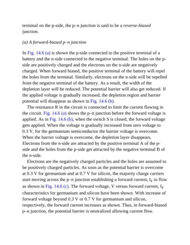
               In Fig. 14.6 (a) is shown the p-side connected to the positive terminal of a
               battery and the n-side connected to the negative terminal. The holes on the p-

               side are positively charged and the electrons on the n-side are negatively
               charged. When forward biased, the positive terminal of the battery will repel
               the holes from the terminal. Similarly, electrons on the n-side will be repelled

               from the negative terminal of the battery. As a result, the width of the
               depletion layer will be reduced. The potential barrier will also get reduced. If

               the applied voltage is gradually increased, the depletion region and barrier
               potential will disappear as shown in Fig. 14.6 (b).

                  The resistance R in the circuit is connected to limit the current flowing in
               the circuit. Fig. 14.6 (a) shows the p–n junction before the forward voltage is

               applied. As in Fig. 14.6 (b), when the switch S is closed, the forward voltage
               gets applied. When the voltage is gradually increased from zero voltage to
               0.3 V, for the germanium semiconductor the barrier voltage is overcome.

               When the barrier voltage is overcome, the depletion layer disappears.
               Electrons from the n-side are attracted by the positive terminal A of the p-

               side and the holes from the p-side get attracted by the negative terminal B of
               the n-side.
                  Electrons are the negatively charged particles and the holes are assumed to

               be positively charged particles. As soon as the potential barrier is overcome
               at 0.3 V for germanium and at 0.7 V for silicon, the majority charge carriers

               start moving across the p–n junction establishing a forward current, I  to flow
                                                                                                  F
               as shown in Fig. 14.6 (c). The forward voltage, V versus forward current, I               F

               characteristics for germanium and silicon have been shown. With increase of

               forward voltage beyond 0.3 V or 0.7 V for germanium and silicon,
               respectively, the forward current increases as shown. Thus, in forward-biased

               p–n junction, the potential barrier is neutralized allowing current flow.

