


Page 961 - Basic Electrical Engineering
P. 961
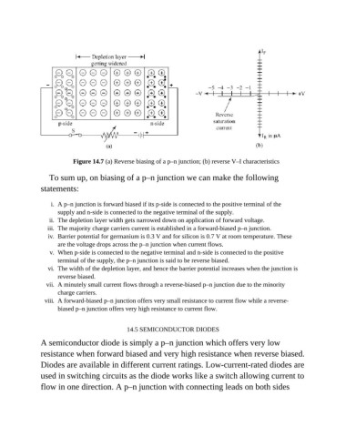
Figure 14.7 (a) Reverse biasing of a p–n junction; (b) reverse V–I characteristics


                  To sum up, on biasing of a p–n junction we can make the following
               statements:


                   i.  A p–n junction is forward biased if its p-side is connected to the positive terminal of the
                     supply and n-side is connected to the negative terminal of the supply.
                  ii.  The depletion layer width gets narrowed down on application of forward voltage.
                  iii.  The majority charge carriers current is established in a forward-biased p–n junction.
                  iv.  Barrier potential for germanium is 0.3 V and for silicon is 0.7 V at room temperature. These
                     are the voltage drops across the p–n junction when current flows.
                   v.  When p-side is connected to the negative terminal and n-side is connected to the positive
                     terminal of the supply, the p–n junction is said to be reverse biased.
                  vi.  The width of the depletion layer, and hence the barrier potential increases when the junction is
                     reverse biased.
                 vii.  A minutely small current flows through a reverse-biased p–n junction due to the minority
                     charge carriers.
                 viii.  A forward-biased p–n junction offers very small resistance to current flow while a reverse-
                     biased p–n junction offers very high resistance to current flow.


                                              14.5 SEMICONDUCTOR DIODES

               A semiconductor diode is simply a p–n junction which offers very low

               resistance when forward biased and very high resistance when reverse biased.
               Diodes are available in different current ratings. Low-current-rated diodes are
               used in switching circuits as the diode works like a switch allowing current to

               flow in one direction. A p–n junction with connecting leads on both sides

