


Page 962 - Basic Electrical Engineering
P. 962
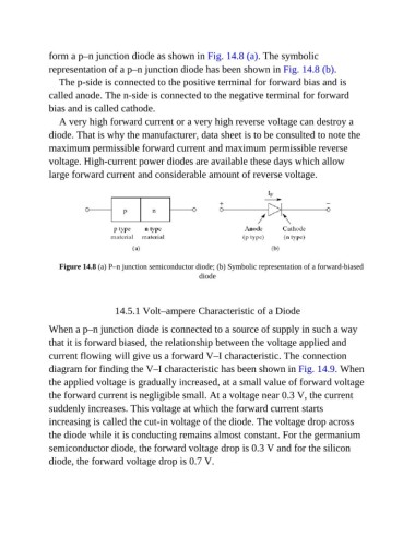
form a p–n junction diode as shown in Fig. 14.8 (a). The symbolic
               representation of a p–n junction diode has been shown in Fig. 14.8 (b).
                  The p-side is connected to the positive terminal for forward bias and is

               called anode. The n-side is connected to the negative terminal for forward
               bias and is called cathode.

                  A very high forward current or a very high reverse voltage can destroy a
               diode. That is why the manufacturer, data sheet is to be consulted to note the

               maximum permissible forward current and maximum permissible reverse
               voltage. High-current power diodes are available these days which allow

               large forward current and considerable amount of reverse voltage.


                  Figure 14.8 (a) P–n junction semiconductor diode; (b) Symbolic representation of a forward-biased
                                                            diode


                                   14.5.1 Volt–ampere Characteristic of a Diode

               When a p–n junction diode is connected to a source of supply in such a way
               that it is forward biased, the relationship between the voltage applied and

               current flowing will give us a forward V–I characteristic. The connection
               diagram for finding the V–I characteristic has been shown in Fig. 14.9. When

               the applied voltage is gradually increased, at a small value of forward voltage
               the forward current is negligible small. At a voltage near 0.3 V, the current

               suddenly increases. This voltage at which the forward current starts
               increasing is called the cut-in voltage of the diode. The voltage drop across

               the diode while it is conducting remains almost constant. For the germanium
               semiconductor diode, the forward voltage drop is 0.3 V and for the silicon
               diode, the forward voltage drop is 0.7 V.

