


Page 968 - Basic Electrical Engineering
P. 968
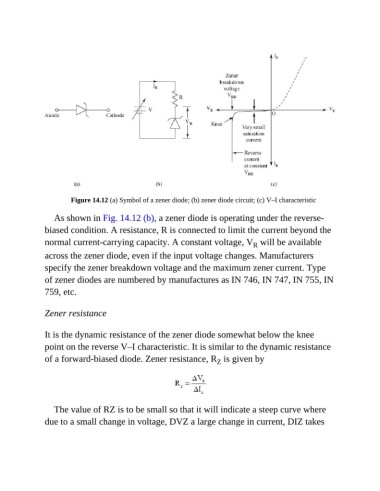
Figure 14.12 (a) Symbol of a zener diode; (b) zener diode circuit; (c) V–I characteristic

                  As shown in Fig. 14.12 (b), a zener diode is operating under the reverse-

               biased condition. A resistance, R is connected to limit the current beyond the
               normal current-carrying capacity. A constant voltage, V  will be available
                                                                                   R
               across the zener diode, even if the input voltage changes. Manufacturers
               specify the zener breakdown voltage and the maximum zener current. Type

               of zener diodes are numbered by manufactures as IN 746, IN 747, IN 755, IN
               759, etc.


               Zener resistance


               It is the dynamic resistance of the zener diode somewhat below the knee
               point on the reverse V–I characteristic. It is similar to the dynamic resistance

               of a forward-biased diode. Zener resistance, R  is given by
                                                                       Z


                  The value of RZ is to be small so that it will indicate a steep curve where
               due to a small change in voltage, DVZ a large change in current, DIZ takes

