


Page 973 - Basic Electrical Engineering
P. 973
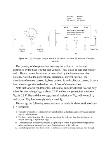
Figure 14.15 (a) Biasing of a n–p–n transistor for normal operation; (b) operation of a n–p–n
                                                          transistor


                  The quantity of charge carriers crossing the emitter to the base in
               controlled by the base–emitter bias voltage. Thus, it can be said that emitter

               and collector current levels can be controlled by the base–emitter bias
               voltage. Note that the conventional direction of current flow i.e., the

               directions of emitter current, I , base current, I  and collector current, I  have
                                                   E
                                                                                                     C
                                                                       B
               been shown opposite to the direction of flow of charge carriers.
                  Note that for a silicon transistor, substantial current will start flowing only
               when the bias voltage V  is about 0.7 V and for the germanium transistor
                                            BE
               V  is 0.3 V. Beyond this voltage, a small variation of V  will control I                 E
                  BE
                                                                                    BE
               and I , and V  has to supply only a small I .
                                BE
                                                                    B
                     C
                  To sum up, the following statements can be made for the operation of a n–
               p–n transistor:

                   i.  The outer layers of n–p–n transistors are called emitter and collector, respectively, the central
                     layer is called the base.
                  ii.  The base–emitter junction, EB is forward biased and the collector–base junction is reverse
                     biased, and V CB  is higher than V BE .
                  iii.  The base section is made very thin and is lightly doped so that majority of the charge carriers
                     (electrons in n–p–n transistor) can move from the emitter to the collector.
                  iv.  Most charge carriers flow from emitter to collector and only a small percentage flow through

