


Page 970 - Basic Electrical Engineering
P. 970
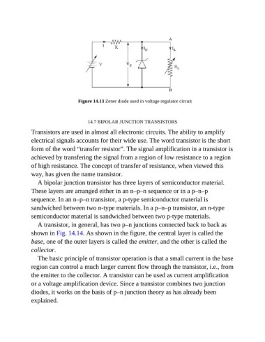
Figure 14.13 Zener diode used in voltage regulator circuit


                                          14.7 BIPOLAR JUNCTION TRANSISTORS

               Transistors are used in almost all electronic circuits. The ability to amplify
               electrical signals accounts for their wide use. The word transistor is the short
               form of the word “transfer resistor”. The signal amplification in a transistor is

               achieved by transfering the signal from a region of low resistance to a region
               of high resistance. The concept of transfer of resistance, when viewed this

               way, has given the name transistor.
                  A bipolar junction transistor has three layers of semiconductor material.

               These layers are arranged either in an n–p–n sequence or in a p–n–p
               sequence. In an n–p–n transistor, a p-type semiconductor material is

               sandwiched between two n-type materials. In a p–n–p transistor, an n-type
               semiconductor material is sandwiched between two p-type materials.
                  A transistor, in general, has two p–n junctions connected back to back as

               shown in Fig. 14.14. As shown in the figure, the central layer is called the
               base, one of the outer layers is called the emitter, and the other is called the

               collector.
                  The basic principle of transistor operation is that a small current in the base
               region can control a much larger current flow through the transistor, i.e., from

               the emitter to the collector. A transistor can be used as current amplification
               or a voltage amplification device. Since a transistor combines two junction

               diodes, it works on the basis of p–n junction theory as has already been
               explained.

