
Page 143 - Fiber Optic Communications Fund
P. 143
124 Fiber Optic Communications
From Eq. (3.103), we have
2 2
ℏ k (7.84 × 10 −26 2
)
E = ℏ − 1 = 2.48 × 10 −19 − J
g −32
2m 2 × 5.59 × 10
r
= 1.93 × 10 −19 J.
3.8 Semiconductor Laser Diode
The light emission in laser diodes is mostly by stimulated emission, whereas that in LEDs is mostly by
spontaneous emission. Laser diodes can emit light at high powers (∼100 mW) and also it is coherent. Because
of the coherent nature of laser output, it is highly directional. The narrower angular spread of the output
beam compared with a LED allows higher coupling efficiency for light coupling to single-mode fibers. An
important advantage of the semiconductor laser is its narrow spectral width, which makes it a suitable optical
source for WDM optical transmission systems (see Chapter 9). A semiconductor laser in its simplest form is
a forward-biased PN junction. Electrons in the conduction band and holes in the valence band are separated
by the band gap and they form a two-band system similar to the atomic system discussed in Sections 3.2
and 3.6. As electrons and holes recombine at the junction, the energy difference is released as photons, as
discussed in Section 3.7.2. To obtain oscillation, optical feedback is required, which is achieved by cleaving
the ends of the laser cavity. Cleaving provides flat and partially reflecting surfaces. Sometimes one reflector
is partially reflecting and used as laser output port and the other has a reflectivity close to unity. By coating
the side opposite the output with a dielectric layer, the reflection coefficient could be close to unity.
3.8.1 Heterojunction Lasers
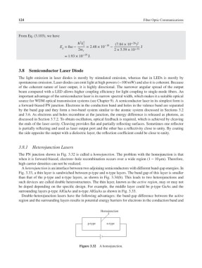
The PN junction shown in Fig. 3.32 is called a homojunction. The problem with the homojunction is that
when it is forward-biased, electron–hole recombination occurs over a wide region (1 − 10 μm). Therefore,
high carrier densities can not be realized.
A heterojunction is an interface between two adjoining semiconductors with different band-gap energies. In
Fig. 3.33, a thin layer is sandwiched between p-type and n-type layers. The band gap of this layer is smaller
than that of the p-type and n-type layers, as shown in Fig. 3.34(b). This leads to two heterojunctions and
such devices are called double heterostructures. The thin layer, known as the active region, may or may not
be doped depending on the specific design. For example, the middle layer could be p-type GaAs and the
surrounding layers p-type AlGaAs and n-type AlGaAs as shown in Fig. 3.33.
Double-heterojunction lasers have the following advantages: the band-gap difference between the active
region and the surrounding layers results in potential energy barriers for electrons in the conduction band and
Homojunction
p-type n-type
Figure 3.32 A homojunction.