
Page 140 - Fiber Optic Communications Fund
P. 140
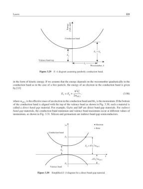
Lasers                                                                             121


                                                   Energy  (Arb. unit)


                                                 Conduction band


                                                                      E 1  > E g
                                                  E g
                              Valence band top
                                                               k 1
                                                                    Wavenumber, k

                              Figure 3.29  E–k diagram assuming parabolic conduction band.


           in the form of kinetic energy. If we assume that the energy depends on the wavenumber quadratically in the
           conduction band as in the case of a free particle, the energy of an electron in the conduction band is given
           by [13]
                                                         2 2
                                                        ℏ k
                                              E = E +      1  ,                             (3.98)
                                               1    g
                                                       2m
                                                          eff,1
           where m eff,1  is the effective mass of an electron in the conduction band and ℏk is the momentum. If the bottom
                                                                       1
           of the conduction band is aligned with the top of the valence band as shown in Fig. 3.30, such a material is
           called a direct band-gap material. For example, GaAs and InP are direct band-gap materials. For indirect
           band-gap materials, the conduction band minimum and valence band maximum occur at different values of
           momentum, as shown in Fig. 3.31. Silicon and germanium are indirect band-gap semiconductors.


                                                  E                     Electron
                                                                        Hole
                                     Conduction band
                                                 E 1


                                                                    2  2
                                                                E g  + ħ k 1 /m eff,1
                                              E g

                                                                               k
                                                                      2  2
                                                                    ‒ħ k 2 /m eff,2
                                                 E 2
                                      Valence band

                             Figure 3.30  Simplified E–k diagram for a direct band-gap material.