
Page 135 - Fiber Optic Communications Fund
P. 135
116 Fiber Optic Communications
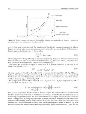
Free electron
Band gap 2
Energy Allowed energy states
Band gap 1
E g1
(Forbidden energy states)
Valence band edge Wavenumer, k
Figure 3.21 Plot of energy vs. wavenumber. The dotted line and solid line correspond to the energy of a free electron
and an electron in a pure semiconductor crystal, respectively.
m eff = 0.07m in the conduction band. The significance of the effective mass can be explained as follows.
0
Suppose an electron in the pure semiconductor crystal is subjected to an external electric field intensity, ,
then the equation of motion is given by Newton’s law,
d(m )
eff
= force = q, (3.95)
dt
where and q are the velocity and charge of an electron, respectively. Note that an electron in a pure semicon-
ductor crystal behaves as if it is a free particle with effective mass m . An electron with m < m experiences
eff eff 0
more acceleration than a free electron subjected to the same force q.
The chance that an electron occupies an energy state E in thermal equilibrium is described by the
Fermi–Dirac function [12]
1
f(E)= , (3.96)
exp [(E − E )∕k T]+ 1
F B
where E is called the Fermi level. From Eq. (3.96), we see that when E = E , f(E)= 0.5. Fig. 3.22 shows
F F
the Fermi–Dirac function as a function of energy. Note that the Fermi function f(E) is not normalized and,
therefore, it is not a probability density function. For an intrinsic semiconductor, the Fermi level is in the
middle of the energy gap, as shown in Fig. 3.23.
For example, at the conduction band bottom, E = E + E and E = E + E ∕2, at temperature T = 300 K,
c
g
F
g
k T ≈ 0.025 eV, and with E = 1eV,
g
B
[ ]
1 E g
f(E )= [ ] ≈ exp − = exp (−20). (3.97)
c
B
exp E g + 1 2k T
2k B T
Thus, at room temperature, the chance that an electron occupies the conduction band is very small and,
therefore, the electrical conductivity of the intrinsic semiconductor is quite low. But the conductivity can be
increased by adding impurity atoms. The basic semiconductor without doping is called an intrinsic semicon-
ductor. Doping consists of adding impurities to the crystalline structure of the semiconductor. For example,
a small amount of group V elements such as arsenic can be added to silicon. Arsenic has five electrons in the
outermost shell; four electrons form a covalent bond with neighboring silicon atoms, as shown in Fig. 3.24,
but there is one electron left over that can not take part in bonding. This fifth electron is very loosely attached