
Page 137 - Fiber Optic Communications Fund
P. 137
118 Fiber Optic Communications
Si
Loose
electron
Si As Si
Si
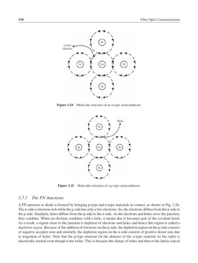
Figure 3.24 Molecular structure of an n-type semiconductor.
Hole
Si
Si Ga Si
Si
Figure 3.25 Molecular structure of a p-type semiconductor.
3.7.1 The PN Junctions
A PN junction or diode is formed by bringing p-type and n-type materials in contact, as shown in Fig. 3.26.
The n-side is electron-rich while the p-side has only a few electrons. So, the electrons diffuse from the n-side to
the p-side. Similarly, holes diffuse from the p-side to the n-side. As the electrons and holes cross the junction,
they combine. When an electron combines with a hole, it means that it becomes part of the covalent bond.
As a result, a region close to the junction is depleted of electrons and holes and hence this region is called a
depletion region. Because of the addition of electrons on the p-side, the depletion region on the p-side consists
of negative acceptor ions and similarly, the depletion region on the n-side consists of positive donor ions due
to migration of holes. Note that the p-type material (in the absence of the n-type material on the right) is
electrically neutral even though it has holes. This is because the charge of holes and that of the lattice cancel