
Page 139 - Fiber Optic Communications Fund
P. 139
120 Fiber Optic Communications
Depletion region after
forward-bias
p-type n-type
* * * + + +
* * * + + +
* * * + + +
* * * + + +
Depletion region before
forward-bias
+ *
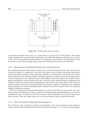
Figure 3.28 The PN junction under forward-bias.
to the negative terminal of the source. As a result, there is a current across the PN junction. The external
voltage counteracts the contact potential and, therefore, the width of the depletion region decreases as shown
in Fig. 3.28. We assume that the external voltage V is less than the contact potential. An external resistor must
be inserted in series with the voltage source to protect the PN junction from an excess current flow.
3.7.2 Spontaneous and Stimulated Emission at the PN Junction
The conduction band and valence band are similar to the excited state and ground state of the atomic system
discussed in Section 3.2, respectively. In the case of the atomic system, an atom in the ground state absorbs
a photon and makes a transition to the excited state. Similarly, in a semiconductor, an electron in the valence
band could jump to the conduction band by absorbing a photon if its energy exceeds the band-gap energy.
As the electron moves to the conduction band, it leaves behind a hole in the valence band. In other words, a
photon is annihilated to create an electron–hole pair. An electron in the conduction band is stimulated to emit
a photon if a photon of the same kind is already present, and it jumps to the valence band. In other words, an
electron combines with a hole, releasing the difference in energy as a photon. An electron in the conduction
band could jump to the valence band spontaneously, whether or not a photon is present. This occurs randomly,
leading to spontaneous emission.
Now let us consider the forward-biased PN junction. As electrons and holes cross the junction, they com-
bine and release the difference in energy as photons. The spontaneously generated photons act as a seed for
stimulated emission. As electrons are lost due to electron–hole recombination, the external voltage source
injects electrons. Thus, the voltage source acts as an electrical pump to achieve population inversion.
3.7.3 Direct and Indirect Band-Gap Semiconductors
Fig. 3.29 shows a plot of energy as a function of wavenumber. Let E be the minimum energy required to
g
excite an electron to the conduction band. If an electron absorbs the energy E > E , the excess energy appears
g
1