
Page 168 - Fiber Optic Communications Fund
P. 168
Optical Modulators and Modulation Schemes 149
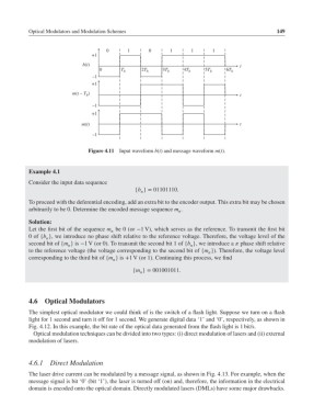
0 1 0 1 1 1
+1
b(t) t
0 T b 2T b 3T b 4T b 5T b 6T b
–1
+1
m(t – T ) t
b
–1
+1
m(t) t
–1
Figure 4.11 Input waveform b(t) and message waveform m(t).
Example 4.1
Consider the input data sequence
{b }= 01101110.
n
To proceed with the deferential encoding, add an extra bit to the encoder output. This extra bit may be chosen
arbitrarily to be 0. Determine the encoded message sequence m .
n
Solution:
Let the first bit of the sequence m be0(or −1 V), which serves as the reference. To transmit the first bit
n
0of {b }, we introduce no phase shift relative to the reference voltage. Therefore, the voltage level of the
n
second bit of {m } is −1 V (or 0). To transmit the second bit 1 of {b }, we introduce a phase shift relative
n
n
to the reference voltage (the voltage corresponding to the second bit of {m }). Therefore, the voltage level
n
corresponding to the third bit of {m } is +1 V (or 1). Continuing this process, we find
n
{m }= 001001011.
n
4.6 Optical Modulators
The simplest optical modulator we could think of is the switch of a flash light. Suppose we turn on a flash
light for 1 second and turn it off for 1 second. We generate digital data ‘1’ and ‘0’, respectively, as shown in
Fig. 4.12. In this example, the bit rate of the optical data generated from the flash light is 1 bit/s.
Optical modulation techniques can be divided into two types: (i) direct modulation of lasers and (ii) external
modulation of lasers.
4.6.1 Direct Modulation
The laser drive current can be modulated by a message signal, as shown in Fig. 4.13. For example, when the
message signal is bit ‘0’ (bit ‘1’), the laser is turned off (on) and, therefore, the information in the electrical
domain is encoded onto the optical domain. Directly modulated lasers (DMLs) have some major drawbacks.