
Page 166 - Fiber Optic Communications Fund
P. 166
Optical Modulators and Modulation Schemes 147
NRZ data m(t)
exp(i2πf t) Fiber link
c
exp{i[2π f c t + k p m(t) + ɵ]}
Laser PM ... ...
exp{i[2π f t + k p m(t)]}
c
Coherent receiver
m(t) DSP front end
exp[i(2π f t)]
c
Laser (LO)
Figure 4.8 Block diagram of a fiber-optic system based on PSK.
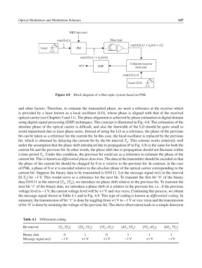
and other factors. Therefore, to estimate the transmitted phase, we need a reference at the receiver which
is provided by a laser known as a local oscillator (LO), whose phase is aligned with that of the received
optical carrier (see Chapters 5 and 11). The phase alignment is achieved by phase estimation in digital domain
using digital signal processing (DSP) techniques. This concept is illustrated in Fig. 4.8. The estimation of the
absolute phase of the optical carrier is difficult, and also the linewidth of the LO should be quite small to
avoid impairment due to laser phase noise. Instead of using the LO as a reference, the phase of the previous
bit can be taken as a reference for the current bit. In this case, the local oscillator is replaced by the previous
bit, which is obtained by delaying the current bit by the bit interval T . This scheme works relatively well
b
under the assumption that the phase shift introduced due to propagation ( in Fig. 4.8) is the same for both the
current bit and the previous bit. In other words, the phase shift due to propagation should not fluctuate within
a time period T . Under this condition, the previous bit could act as a reference to estimate the phase of the
b
current bit. This is known as differential phase detection. The data at the transmitter should be encoded so that
the phase of the current bit should be changed by 0 or relative to the previous bit. In contrast, in the case
of PSK, a phase of 0 or is encoded relative to the absolute phase of the optical carrier corresponding to the
current bit. Suppose the binary data to be transmitted is 010111. Let the message signal m(t) in the interval
[0, T ] be −1 V. This would serve as a reference for the next bit. To transmit the first bit ‘0’ of the binary
b
data 010111 in the interval [T , 2T ], we introduce no phase shift relative to the previous bit. To transmit the
b b
next bit ‘1’ of the binary data, we introduce a phase shift of relative to the previous bit, i.e., if the previous
voltage level is −1 V, the current voltage level will be +1 V and vice versa. Continuing this process, we obtain
the message signal shown in Table 4.1 and in Fig. 4.9. This type of coding is known as differential coding.In
summary, the transmission of bit ‘1’ is done by toggling from +1 V to −1 V or vice versa and the transmission
of bit ‘0’ is done by retaining the voltage of the previous bit. The above observation leads to a simple detection
Table 4.1 Differential coding.
Bit interval [T , 2T ] [2T , 3T ] [3T , 4T ] [4T , 5T ] [5T , 6T ] [6T , 7T ]
b b b b b b b b b b b b
Binary data 0 1 0 1 1 1
Message signal m(t) −1 V +1 V +1 V −1 V +1 V −1 V