
Page 164 - Fiber Optic Communications Fund
P. 164
Optical Modulators and Modulation Schemes 145
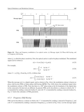
m(t) 1 1 0 1 0 1 1 1
Message signal
t
s(t) (a) 180° phase jump
PSK
t
s(t) (b)
FSK
t
(c)
Figure 4.6 Phase and frequency modulation of an optical carrier. (a) Message signal, (b) Phase-shift keying, and
(c) Frequency-shift keying.
where k is called the phase sensitivity. Now, the optical carrier is said to be phase modulated. The modulated
p
signal can be written as
s(t)= A cos [2f t + k m(t)]. (4.25)
c
p
For example,
{
−V for bit ‘1’
m(t)= , (4.26)
V for bit ‘0’
where V = ∕(2k ). From Eq. (4.25), it follows that
p
{
( )
A sin 2f t for bit ‘1’
c
s(t)= . (4.27)
−A sin (2f t) for bit ‘0’
c
When the message m(t) is a digital signal, such as shown in Fig. 4.6(a), the modulation scheme is known as
phase-shift keying (PSK) or binary phase-shift keying (BPSK). Fig. 4.6(b) shows the modulated signal when
∘
the modulation scheme is PSK. Note that there is a 180 phase jump at the bit boundaries if the digital data
in the consecutive bit intervals are different. In general, PSK can be described as a scheme in which a bit ‘1’
is transmitted by sending a sinusoid of phase and a bit ‘0’ is transmitted by sending a sinusoid of phase .
1 2
Fig. 4.7 shows the schematic of PSK generation.
4.5.3 Frequency-Shift Keying
FSK can be described as a scheme in which a bit ‘1’ is transmitted by sending a sinusoid of frequency f and
1
a bit ‘0’ is transmitted by sending a sinusoid of frequency f , as shown in Fig. 4.6(c). Let the message signal
2