
Page 167 - Fiber Optic Communications Fund
P. 167
148 Fiber Optic Communications
+1V
m(t)
0 T b 2T b 3T b 4T b 5T b 6T b 7T b
–1V
Figure 4.9 The DPSK signal corresponding to the binary data of Table 4.1.
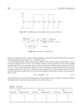
NRZ data
m(t) Phase DPSK signal
b(t) XOR
modulator Acos[2π f t + k m(t)]
p
c
Delay T Acos(2π f t)
c
b
Figure 4.10 Generation of a DPSK signal.
scheme: take a product of the current bit (after demodulation) with the previous bit. If the product is negative,
the transmitted data at the current bit is ‘1’. Otherwise, it is ‘0’.
The differential encoding can be realized using a XOR gate and a delay circuit as shown in Fig. 4.10. Let
us assign a voltage level of +1 V and −1 V to the logic levels of 1 and 0, respectively. Let m(t) be the encoded
message signal. If the incoming binary data b(t) to be transmitted is 0 and the previous message bit (of m(t))
is 0 (or −1 V), the current message bit will also be 0 since we introduce no phase shift relative to the previous
message bit. If the binary data b(t) is 1 and the previous message bit is 0 (1), the current bit will be 1 (0) since
we need to introduce a phase shift (or inversion of the amplitude) with respect to the previous message bit.
Thus, we have
m(t)= b(t) ⊕ m(t − T ), (4.33)
b
where ⊕ denotes the exclusive OR (XOR) operation. The truth table is shown in Table 4.2 and the waveforms
for the input data b(t) and the message signal m(t) are shown in Fig. 4.11.
Table 4.2 Truth table.
b(t) m(t − T ) m(t)
b
Logic level Voltage level (V) Logic level Voltage level (V) Logic level Voltage level (V)
0 −1 0 −1 0 −1
0 −1 1 1 1 1
1 1 0 −1 1 1
1 1 1 1 0 −1