
Page 289 - Fiber Optic Communications Fund
P. 289
270 Fiber Optic Communications
about 9 THz and a gain ripple ΔG of about 1.5 dB. Owing to the non-resonant character of the NTWA, it was
found to be less sensitive to temperature, bias current, and input signal polarization fluctuations compared
with the FPA.
In order to reduce the reflectivities of the end facets, AR coatings may be applied to the end facets. The
optical field transmission at a dielectric interface is accompanied by reflection. However, if we deposit an
intermediate layer (AR coating) between the two dielectric media, it is possible to avoid reflections. In the
following section, the principle behind the AR coating is discussed.
6.6.3 AR Coating
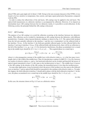
The purpose of an AR coating is to avoid the reflection occurring at the interface between two dielectric
media. This reflection can be avoided by introducing an AR coating between the dielectrics with different
permittivities. Consider a three-layered dielectric medium as shown in Fig. 6.13. The optical field incident
from the left gets partially reflected at the interface 1 and the rest is transmitted. Let the reflected field at
the interface 1 be . At the interface 2, the field gets partially reflected again. Let the reflected field at the
1
interface 2 arriving at interface 1 be . If the reflected fields add destructively, there will be no reflection to
2
the left of the interface 1, i.e., + = 0. For destructive interference, the phase accumulated over a round
2
1
trip in the middle layer should be (2l + 1), l = 0, ±1, ±2, … The acquired phase in a round trip is
4n (2l + 1) 0
2
= 2k = =(2l + 1) or = , (6.137)
2
0 4n 2
where k is the propagation constant of the middle layer with refractive index n , is the free-space wave-
2 2 0
length, and is the width of the middle layer. Thus, by introducing a coating of width (2l + 1) ∕4n between
0 2
two media of refractive indices n and n , the backward reflection can be avoided and therefore the power of
1 3
optical signal transmitted to layer 3 is the same as the incident power to layer 1. The middle layer is known
as the AR coating. In the absence of the AR coating, the transmitted power is less than the incident power.
In some other application, it may be desired to have the power of the incident wave the same as the reflected
wave at interface 1 and no optical field should be transmitted to the medium with refractive index n .Tomake
3
this happen, the field reflected at interface 2 should add in-phase with the field reflected at interface 1. In this
case, the phase accumulated over a round trip in the middle layer should be 2l, l = 0, ±1, ±2, … , i.e.,
4n 2 l 0
= = 2l or = . (6.138)
2n
0 2
In this case, the structure shown in Fig. 6.13 acts as a dielectric mirror.
Interface Interface
1 2
n 1 n 2 n 3
ψ 1 ψ 2
Incident Transmitted
wave wave
w
Figure 6.13 Three-layered dielectric structure.