
Page 65 - GIGABYTE Service Manual-v3.0-110101
P. 65
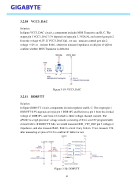
3.2.10  VCC3_DAC


                   Solution:
                   In figure VCC3_DAC circuit, a component includes MOS Transistor and R, C. The

                   output pin 1 VCC3_DAC 3.3V depends on input pin 3, 3VDUAL and control gate pin 2
                   from the voltage +12V. If VCC3_DAC fail , we can  measure control gate pin 2
                   voltage +12V or   resistor R146 , otherwise measure impedance on all pins of Q20 to
                   confirm whether MOS Transistor is defected.


                                                Figure 3-19: VCC3_DAC

                   3.2.11  DDRVTT


                   Solution:
                   In figure DDRVTT circuit, components include regulator and R, C. The output pin 4
                   DDRVTT 0.9V depends on input pin 1 DDR18V and Reference pin 3 from the divided
                   voltage of DDR18V, and from U14 which is three voltage channel console. The

                   uP6262 is a high precision voltage console consisting of three sets I2C programmable
                   current DACs. If DDRVTT fails, we would measure DDR_VTT_REF pin 3 voltage or
                   impedance, and also measure R441, R443 to check if any broken. If not, measure U14
                   after measuring all pins of U12 to confirm IC defect or not.


                                                 Figure 3-20: DDRVTT


                                                            43