
Page 63 - GIGABYTE Service Manual-v3.0-110101
P. 63
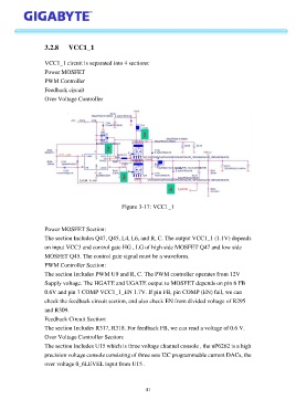
3.2.8     VCC1_1


                   VCC1_1 circuit is separated into 4 sections:
                   Power MOSFET

                   PWM Controller
                   Feedback circuit
                   Over Voltage Controller


                                                  Figure 3-17: VCC1_1


                   Power MOSFET Section:
                   The section Includes Q47, Q45, L4, L6, and R, C. The output VCC1_1 (1.1V) depends
                   on input VCC3 and control gate HG , LG of high side MOSFET Q47 and low side
                   MOSFET Q45. The control gate signal must be a waveform.

                   PWM Controller Section:
                   The section Includes PWM U9 and R, C. The PWM controller operates from 12V
                   Supply voltage. The HGATE and UGATE output to MOSFET depends on pin 6 FB
                   0.6V and pin 7 COMP VCC1_1_EN 1.7V. If pin FB, pin COMP (EN) fail, we can

                   check the feedback circuit section, and also check EN from divided voltage of R295
                   and R309.
                   Feedback Circuit Section:
                   The section Includes R317, R318. For feedback FB, we can read a voltage of 0.6 V.

                   Over Voltage Controller Section:
                   The section Includes U15 which is three voltage channel console , the uP6262 is a high
                   precision voltage console consisting of three sets I2C programmable current DACs, the
                   over voltage 0_6LEVEL input from U15 .


                                                            41