
Page 59 - GIGABYTE Service Manual-v3.0-110101
P. 59
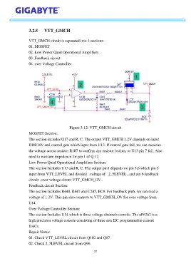
3.2.5     VTT_GMCH


                   VTT_GMCH circuit is separated into 4 sections:
                   01. MOSFET

                   02. Low Power Quad Operational Amplifiers
                   03. Feedback circuit
                   04. over Voltage Controller


                                            Figure 3-12: VTT_GMCH circuit
                   MOSFET Section:
                   The section includes Q17 and R, C. The output VTT_GMCH 1.2V depends on input

                   DDR18V and control gate which input from U13. If control gate fail, we can measure
                   the voltage across resistor R107 to confirm any resistor broken, or U13 pin 7 fail. Also
                   need to measure impedance for pin 1 of Q 17.
                   Low Power Quad Operational Amplifiers Section:
                   The section Includes U13 and R, C. The output pin1 depends on pin 5,6 which pin 5

                   input from VTT_LEVEL and divided  voltage of   2_5LEVEL , and pin 6 feedback
                   circuit , over voltage circuit VTT_GMCH_OV .
                   Feedback circuit Section:

                   The section Includes R440, R447 and C245, EC8. For feedback pin6, we can read a
                   voltage of 1.2V. This pin also connects to VTT_GMCH_OV for over voltage from
                   U14.
                   Over Voltage Controller Section:
                   The section Includes U14 which is three voltage channels console. The uP6262 is a

                   high precision voltage console consisting of three sets I2C programmable current
                   DACs.
                   Repair Notes:

                   01. Check VTT_LEVEL circuit from Q102 and Q87
                   02. Check 2_5LEVEL circuit from Q96.

                                                            37