
Page 64 - GIGABYTE Service Manual-v3.0-110101
P. 64
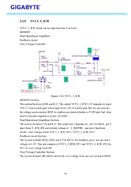
3.2.9     VCC1_1_ICH


                   VCC1_1_ICH circuit can be separated into 4 sections:
                   MOSFET

                   Dual Operational Amplifiers
                   Feedback circuit
                   Over Voltage Controller


                                               Figure 3-18: VCC1_1_ICH

                   MOSFET Section:
                   The section Includes Q106 and R, C. The output VCC1_1_ICH 1.1V depends on input
                   VCC1_5 and control gate which input from U19. If control gate fail, we can measure
                   the voltage across resistor R385 to confirm any resistor broken or U189 pin1 fail. Also
                   need to measure impedance on pin 1of Q106.

                   Dual Operational Amplifiers Section:
                   The section Includes U19 and R, C. The output pin 7 depends on  pin 5,6 which  pin 5
                   input from V_ICH_EN and divided voltage of   2_5LEVEL , and pin 6 feedback

                   circuit , over voltage circuit VCC1_1_ICH_OV1, VCC1_1_ICH_OV2 .
                   Feedback circuit Section:
                   The section Includes R542, R541 and C274, EC14. For feedback pin 6, we can read a
                   voltage of 1.1V. This pin connects to VCC1_1_ICH_OV1 and VCC1_1_ICH_OV2 by
                   D13 for over voltage from SB.

                   Over Voltage Controller Section:
                   The section Includes SB which controls the over voltage from end-user setting in BIOS.


                                                            42