
Page 62 - GIGABYTE Service Manual-v3.0-110101
P. 62
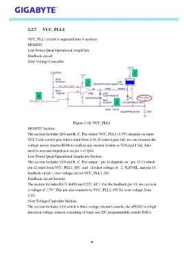
3.2.7     VCC_PLL1


                   VCC_PLL1 circuit is separated into 4 sections:
                   MOSFET

                   Low Power Quad Operational Amplifiers
                   Feedback circuit
                   Over Voltage Controller


                                                Figure 3-16: VCC_PLL1
                   MOSFET Section:
                   The section Includes Q16 and R, C. The output VCC_PLL1 (1.5V) depends on input

                   VCC3 and control gate which input from U18. If control gate fail, we can measure the
                   voltage across resistor R106 to confirm any resistor broken or U18 pin14 fail. Also
                   need to measure impedance on pin 1 of Q16.
                   Low Power Quad Operational Amplifiers Section:
                   The section Includes U18 and R, C. The output  pin 14 depends on   pin 12,13 which

                   pin 12 input from VCC_PLL1_EN   and  divided voltage of  2_5LEVEL, and pin 13
                   feedback circuit , over voltage circuit VCC_PLL1_OV.
                   Feedback circuit Section:

                   The section Includes R471, R459 and C257, EC7. For the feedback pin 13, we can read
                   a voltage of 1.5V. This pin also connects to VCC_PLL1_OV for over voltage from
                   U10.
                   Over Voltage Controller Section:
                   The section Includes U10 which is three voltage channel console, the uP6262 is a high

                   precision voltage console consisting of three sets I2C programmable current DACs.


                                                            40