
Page 58 - GIGABYTE Service Manual-v3.0-110101
P. 58
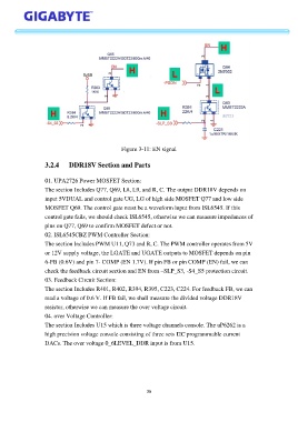
Figure 3-11: EN signal


                   3.2.4     DDR18V Section and Parts


                   01. UPA2726 Power MOSFET Section:
                   The section Includes Q77, Q69, L8, L9, and R, C. The output DDR18V depends on

                   input 5VDUAL and control gate UG, LG of high side MOSFET Q77 and low side
                   MOSFET Q69. The control gate must be a waveform input from ISL6545. If this
                   control gate fails, we should check ISL6545, otherwise we can measure impedances of

                   pins on Q77, Q69 to confirm MOSFET defect or not.
                   02. ISL6545CBZ PWM Controller Section:
                   The section Includes PWM U11, Q73 and R, C. The PWM controller operates from 5V
                   or 12V supply voltage, the LGATE and UGATE outputs to MOSFET depends on pin
                   6-FB (0.6V) and pin 7- COMP (EN 1.7V). If pin FB or pin COMP (EN) fail, we can

                   check the feedback circuit section and EN from –SLP_S3, -S4_S5 protection circuit.
                   03. Feedback Circuit Section:
                   The section Includes R401, R402, R394, R395, C223, C224. For feedback FB, we can

                   read a voltage of 0.6 V. If FB fail, we shall measure the divided voltage DDR18V
                   resistor, otherwise we can measure the over voltage circuit.
                   04. over Voltage Controller:
                   The section Includes U15 which is three voltage channels console. The uP6262 is a
                   high precision voltage console consisting of three sets I2C programmable current

                   DACs. The over voltage 0_6LEVEL_DDR input is from U15.


                                                            36