
Page 54 - GIGABYTE Service Manual-v3.0-110101
P. 54
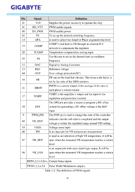
Pin        Signal                              Definition

                    21           VCC        Supplies the power necessary to operate the chip
                    41        EN_VTT        PWM enable signals
                    40       EN_PWR         PWM enable power

                    42           FS         To set up the desired switching frequency
                    14          APA         is used to adjust the Adaptive Phase alignment trip level
                                            COMP is tied back to FB through an external R-C
                    15          COMP
                                            network to compensate the regulator
                    20          TCOMP       Temperature compensation scaling input
                                            Use this pin to set up the desired start-up oscillator
                    43            SS
                                            frequency

                    12          DAC         Digital-to Analog Converter
                    13          REF         Reference voltage
                    44          OVP         Over voltage protection(NC)

                                            FB can set the load line (droop). The droop scale factor is
                    16           FB
                                            set by the ratio of the ISEN resistors
                                            IMON is a current output of the average of the sum of
                    11          IMON
                                            each phase’s sensed current

                                            VDIFF is the amplifier’s output and the input to the
                    17         VDIFF
                                            regulation and protection circuitry
                                            The OFS pin provides a means to program a DC offset

                    10          OFS         current for generating a DC offset voltage at the REF
                                            input
                     9       PWM_PSI      The PSI# pin is used to change the state of the controller
                                            indicates that the soft-start is completed and the output
                    45       VR_RDY
                                            voltage is within the regulated range around VID setting
                    19         VSEN         Voltage sense input
                    48          TM          Is an input pin for VR temperature measurement.

                                            is used as an indication of high VR temperature, It will be
                    47        VR_HOT        open when the measured VR temperature reaches a certain
                                            level
                                            is an output pin with open-drain logic output, It will be

                    46        VR_FAN        open when the measured VR temperature reaches a certain
                                            level


                          ISEN1,2,3,4,5,6/+,- Current Sense inputs
                          PWM1,2,3,4,5,6      Pulse Width Modulation outputs,

                                        Table 3-2: The definition of PWM signals


                                                            32