
Page 51 - GIGABYTE Service Manual-v3.0-110101
P. 51
Chapter 3 VCORE and Chipsets Voltage
3.1 VCORE
3.1.1 VCORE Voltage
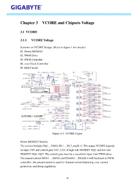
Sections for VCORE Design: (Refer to figure 1 for circuits)
01. Power MOSFET
02. PWM Drive
03. PWM Controller
04. over Clock Controller
05. DES Circuit
Figure 3-1: VCORE Figure
Power MOSFET Section:
The section Includes DQ1…DQ18, DL1…DL7, and R, C. The output VCORE depends
on input VIN and control gate UG1, LG1 of high side MOSFET DQ1 and low side
MOSFET DQ4, DQ7. The control gate must be a waveform input from PWM drive.
The sensed current ISEN1 …ISEN6 and PHASE1…PHASE 6 will feedback to PWM
controller , the sensed current is used for channel current balancing, over current
protection, and droop regulation.
29