
Page 47 - GIGABYTE Service Manual-v3.0-110101
P. 47
+1.2V_VBAT
VBAT on always
+3.3V_DUAL
+5V_DUAL
+1.2V_DUAL
+3.3V_PLL_DUAL
determined by motherboard implemention (min= 1 ms)
PWRGD_SB
Standby Standby clocks will drive stable outputs within 10ms after PWRGD_SB deassertion
clocks
(SUSCLK,
BUF_25MHZ)
Fixed CK8 delay guarantees system clocks are stable
SLP_S5#
+2.5V_SUS Memory power valid input delay
+1.25V_VTT_SUS determined by motherboard implementation (min=1ms)
MEM_VLD#
( connect compement to ps_on ) -5ms fixed CK8 delay
SLP_ S3#
+12V,+5V,+3.3V
+1.2V,+3.3V_PLL,
+2.5V_VCCA 100~500ms silver box PWROK delay plus any motherboard implementation specific delays
System clocks will drive stable outputs within 10ms after PWRGD_CK8 deassertion
PWRGD_CK8
CPU,PCI,LPC,
AGP,SATA,
Internal
Clocks Fixed CK8 delay guarantees system clocks are stable
CPUVDD_EN
Standby clocks will drive stable outputs within 10ms after PWRGD_SB deassertion
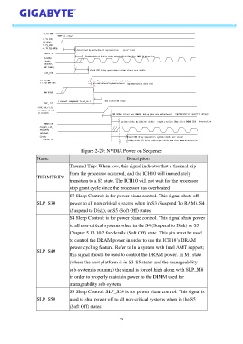
Figure 2-29: NVDIA Power on Sequence
Name Description
Thermal Trip: When low, this signal indicates that a thermal trip
from the processor occurred, and the ICH10 will immediately
THRMTRIP#
transition to a S5 state. The ICH10 will not wait for the processor
stop grant cycle since the processor has overheated.
S3 Sleep Control: is for power plane control. This signal shuts off
SLP_S3# power to all non-critical systems when in S3 (Suspend To RAM), S4
(Suspend to Disk), or S5 (Soft Off) states.
S4 Sleep Control: is for power plane control. This signal shuts power
to all non-critical systems when in the S4 (Suspend to Disk) or S5
Chapter 5.13.10.2 for details (Soft Off) state. This pin must be used
to control the DRAM power in order to use the ICH10’s DRAM
power-cycling feature. Refer to In a system with Intel AMT support;
SLP_S4#
this signal should be used to control the DRAM power. In M1 state
(where the host platform is in S3-S5 states and the manageability
sub-system is running) the signal is forced high along with SLP_M#
in order to properly maintain power to the DIMM used for
manageability sub-system.
S5 Sleep Control: SLP_S5# is for power plane control. This signal is
SLP_S5# used to shut power off to all non-critical systems when in the S5
(Soft Off) states.
25