
Page 298 - FUNDAMENTALS OF COMPUTER
P. 298
NPP
298 Fundamentals of Computers NPP
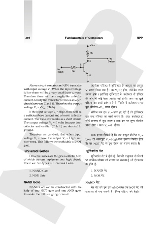
+VCC
RC
V2
C Output
B
V1
Input RB
E
Above circuit contains an NPN transistor Cnamo³V n[anW _| Q´>m§{OñQ>a Ho$ AmYma na BZnwQ>
with input voltage V . When the input voltage V àXmZ {H$`m J`m h¡Ÿ& O~ V = 0 hmoJm, V~ ~og H$a§Q>
1
1
1
is low there will be a very small base current. ZJÊ` hmoJmŸ& Bgr{bE Q´>m§{OñQ>a Ho$ H$boŠQ>a go E{_Q>a
Therefore there will be a negligible collector
current. Ideally the transistor works as an open H$s Amoa ^r H$moB© Ymam àdm{hV Zht hmoJrŸ& AV… `h Iwbo
circuit between C and E. Therefore the output n[anW H$m H$m`© H$aoJmŸ& Eogr pñW{V _| H$boŠQ>a C na
voltage V = +V (High). nyam dmoëQ>oO +V àmßV hmoJmŸ&
CC
2
CC
If the input voltage V = High, there will be bo{H$Z O~ h_ V = CÀM (1) XoVo h¢ Vmo Q´>m§{OñQ>a
1
1
a sufficient base current and a heavy collector EH$ ~ÝX n[anW H$m H$m`© H$aVm h¡Ÿ& AV… H$boŠQ>a C
current. The transistor works as a short circuit.
The output voltage V = 0 volts because both grYo J«mCÊS> go Ow‹S> OmEJmŸ& AV… Bg na eyÝ` dmoëQ>oO
2
collector and emitter (C & E) are shorted to àmßV hmoJmŸ& AV… V = 0 hmoJmŸ&
2
ground.
Therefore we conclude that when input AV… h‘mam {ZîH$f© h¡ {H$ O~ BZnwQ> dmoëQ>oO V =
1
voltage V = Low, the output V = High and Low, Vmo AmCQ>nwQ> V = High VWm BgH$m {dnarV hmoVm
2
1
vice-versa. This follows the truth table of NOT 2
gate. h¡& ¶h NOT JoQ> Ho$ Q¯>W Q>o~b H$m nmbZ H$aVm h¡&
Universal Gates `y{Zdg©b JoQ>
Universal Gates are the gates with the help `y{Zdg©b JoQ> do hmoVo h¢, {OZH$s ghm`Vm go {H$gr
of which we can implement any logic circuit. ^r Vm{H©$H$ n[anW H$mo ~Zm`m Om gH$Vm h¡Ÿ& `o Xmo àH$ma
There are two types of Universal Gates: Ho$ hmoVo h¢…
1. NAND Gate 1. NAND JoQ
2. NOR Gate 2. NOR JoQ
NAND Gate NAND JoQ>
NAND Gate can be constructed with the Z|S> JoQ> H$mo h_ EH$ AND VWm EH$ NOT JoQ> H$s
help of one NOT gate and one AND gate. ghm`Vm go ~Zm gH$Vo h¢Ÿ& {ZåZ n[anW H$mo XoImo…
Consider the following logic circuit: