
Page 299 - FUNDAMENTALS OF COMPUTER
P. 299
NPP
NPP Number System, Boolean Algebra and Logic Circuits 299
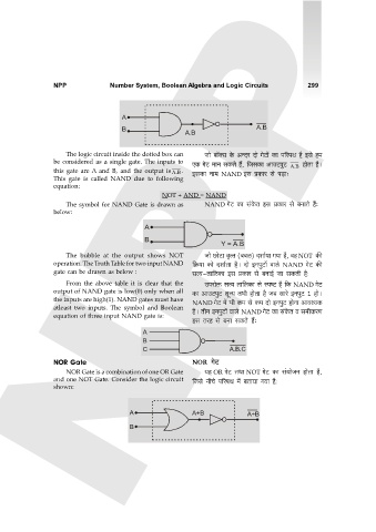
A
B A.B A.B
The logic circuit inside the dotted box can Omo ~m°Šg Ho$ AÝXa Xmo JoQ>m| H$m n[anW h¡ Bgo h_
be considered as a single gate. The inputs to EH$ JoQ> _mZ gH$Vo h¢, {OgH$m AmCQ>nwQ A.B hmoVm h¡Ÿ&
this gate are A and B, and the output is A.B . BgH$m Zm_ NAND Bg àH$ma go n‹S>m…
This gate is called NAND due to following
equation:
NOT + AND = NAND
The symbol for NAND Gate is drawn as NAND JoQ> H$m g§Ho$V Bg àH$ma go ~ZmVo h¢…
below:
A
B
Y = A.B
The bubble at the output shows NOT Omo N>moQ>m d¥ËV (~~c) Xem©`m J`m h¡, dh NOT H$s
operation. The Truth Table for two input NAND {H«$`m H$mo Xem©Vm h¡Ÿ& Xmo BZnwQ>m| dmco NAND JoQ> H$s
gate can be drawn as below : gË`-Vm{cH$m Bg àH$ma go ~ZmB© Om gH$Vr h¡:
From the above table it is clear that the Cnamoº$ gË` Vm{bH$m go ñnîQ> h¡ {H$ NAND JoQ>
output of NAND gate is low(0) only when all H$m AmCQ>nwQ> eyÝ` V^r hmoVm h¡ O~ gmao BZnwQ> 1 hmoŸ&
the inputs are high(1). NAND gates must have NAND JoQ> _| ^r H$_ go H$_ Xmo BZnwQ> hmoZm Amdí`H$
atleast two inputs. The symbol and Boolean
equation of three input NAND gate is: h¡Ÿ& VrZ BZnwQ>m| dmbo NAND JoQ> H$m g§Ho$V d g_rH$aU
Bg Vah go ~Zm gH$Vo h¢…
A
B
C A.B.C
NOR Gate NOR> JoQ>
NOR Gate is a combination of one OR Gate `h OR JoQ> VWm NOT JoQ> H$m g§`moOZ hmoVm h¡,
and one NOT Gate. Consider the logic circuit {Ogo ZrMo n[anW _| ~Vm`m J`m h¡:
shown:
A A+B A+B
B