
Page 296 - FUNDAMENTALS OF COMPUTER
P. 296
NPP
296 Fundamentals of Computers NPP
When A or B is at +5V then any of the O~ A `m B _| go {H$gr EH$ na ^r +5V XoVo h¢ Vmo
diodes will be forward biased. That diode will H$moB© ^r EH$ S>m`moS>, {Og na +5V {X`m J`m h¡, \$madS>©
work as a Short Circuit. Therefore Y will be at ~m`g hmo OmEJm VWm ~ÝX n[anW H$m H$m`© H$aoJmŸ& AV…
+5V. When both the switches (Diodes) are at Y na dht +5V àmßV hmoJmŸ& O~ XmoZm| pñdMog (S>m`moS²>g)
+5V then also Y=+5V. When A = B = 0 then both +5V na hmoVo h¢ Vmo ^r Y = +5V hmoVm h¡Ÿ& O~ A = B
= 0 Vmo XmoZm| S>m`moS²>g AmonZ g{H©$Q> Ho$ ê$n _| H$m`© H$a|Jo
the diodes will work as open circuit and output VWm AmCQ>nwQ> Y = 0 hmoJmŸ& Bg àH$ma Y H$m _mZ 1
Y = 0. Thus, Y is 1 when Atleast one input is 1.
hmoVm h¡ O~ H$_ go H$_ 1 BZnwQ> H$m _mZ 1 hmoVm h¡Ÿ&
The output Y is Zero when both inputs A and Y na 0 Volts V^r àmßV hmoJm O~ XmoZm| A = B = 0 hmoŸ&
B are Zero. Thus, the above circuit follows the AV… `h n[anW OR JoQ> H$s gË`-Vm{bH$m H$m nmbZ
truth table of OR Gate. H$aVm h¡Ÿ&
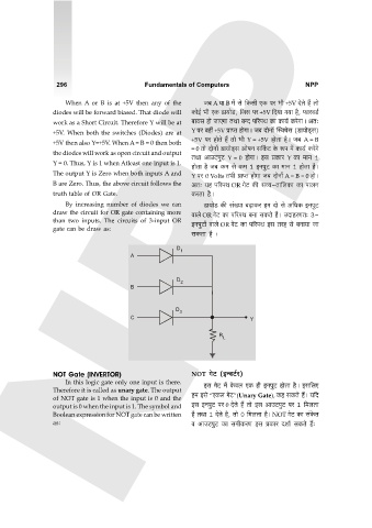
By increasing number of diodes we can S>m`moS> H$s g§»`m ~‹T>mH$a h_ Xmo go A{YH$ BZnwQ>
draw the circuit for OR gate containing more dmbo OR JoQ> H$m n[anW ~Zm gH$Vo h¡Ÿ& CXmhaUV… 3-
than two inputs. The circuits of 3-input OR BZnwQ>m| dmbo OR JoQ> H$m n[anW Bg Vah go ~Zm`m Om
gate can be draw as:
gH$Vm h¡ …
D 1
A
D 2
B
D 3
C Y
R
L
NOT Gate (INVERTOR) NOT JoQ> (BÝdQ>©a)
In this logic gate only one input is there. Bg JoQ> _| Ho$db EH$ hr BZnwQ> hmoVm h¡Ÿ& Bg{bE
Therefore it is called as unary gate. The output
of NOT gate is 1 when the input is 0 and the h_ Bgo “EH$b JoQ>”(Unary Gate), H$h gH$Vo h¢Ÿ& `{X
output is 0 when the input is 1. The symbol and Bg BZnwQ> na 0 XoVo h¢ Vmo Bg AmCQ>nwQ> na 1 {_bVm
Boolean expression for NOT gate can be written h¡ VWm 1 XoVo h¡, Vmo 0 {_bVm h¡Ÿ& NOT JoQ> H$m g§Ho$V
as: d AmCQ>nwQ> H$m g_rH$aU Bg àH$ma Xem© gH$Vo h¢…