
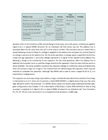
Page 106 - Handout of Computer Architecture (1)..
P. 106
dynamic refers to this tendency of the stored charge to leak away, even with power continuously applied.
               Figure 5.2a  is  a  typical  DRAM  structure  for  an  individual  cell  that  stores  one  bit.  The  address  line  is
               activated when the bit value from this cell is to be read or written. The transistor acts as a switch that is
               closed (allowing current to flow) if a voltage is applied to the address line and open (no current flows) if
               no voltage is present on the address line. For the write operation, a voltage signal is applied to the bit line;
               a high volt age represents 1, and a low voltage represents 0. A signal is then applied to the address line,
               allowing a charge to be transferred to the capacitor. For the read operation, when the address line is
               selected, the transistor turns on and the charge stored on the capacitor is fed out onto a bit line and to a
               sense amplifier. The sense amplifier compares the capacitor voltage to a reference value and determines
               if the cell contains a logic 1 or a logic 0. The readout from the cell discharges the capacitor, which must be
               restored to complete the operation. Although the DRAM cell is used to store a single bit (0 or 1), it is
               essentially an analog device.

               The capacitor can store any charge value within a range; a thresh old value determines whether the charge
               is interpreted as 1 or 0. static ram In contrast, a static RAM (SRAM) is a digital device that uses the same
               logic elements used in the processor. In a SRAM, binary values are stored using traditional flip-flop logic-
               gate configurations (see Chapter 11 for a description of flip-flops). A static RAM will hold its data as long
               as power is supplied to it. Figure 5.2b is a typical SRAM structure for an individual cell. Four transistors
               (T1, T2, T3, T4) are cross connected in an arrangement that produces a stable logic


                                                             106