
Page 15 - Handout of Computer Architecture (1)..
P. 15
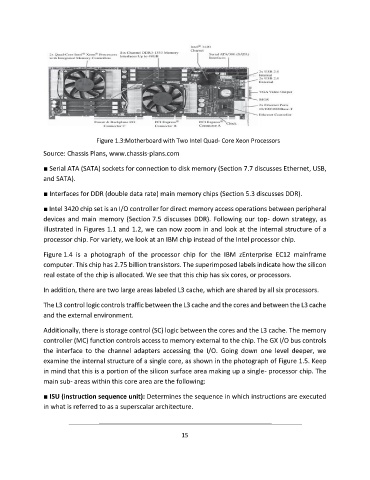
Figure 1.3:Motherboard with Two Intel Quad- Core Xeon Processors

               Source: Chassis Plans, www.chassis-plans.com

               ■ Serial ATA (SATA) sockets for connection to disk memory (Section 7.7 discusses Ethernet, USB,
               and SATA).

               ■ Interfaces for DDR (double data rate) main memory chips (Section 5.3 discusses DDR).

               ■ Intel 3420 chip set is an I/O controller for direct memory access operations between peripheral
               devices and main memory (Section 7.5 discusses DDR). Following our top- down strategy, as

               illustrated in Figures 1.1 and 1.2, we can now zoom in and look at the internal structure of a
               processor chip. For variety, we look at an IBM chip instead of the Intel processor chip.

               Figure 1.4  is  a  photograph  of  the  processor  chip  for  the  IBM  zEnterprise  EC12  mainframe
               computer. This chip has 2.75 billion transistors. The superimposed labels indicate how the silicon
               real estate of the chip is allocated. We see that this chip has six cores, or processors.

               In addition, there are two large areas labeled L3 cache, which are shared by all six processors.

               The L3 control logic controls traffic between the L3 cache and the cores and between the L3 cache
               and the external environment.


               Additionally, there is storage control (SC) logic between the cores and the L3 cache. The memory
               controller (MC) function controls access to memory external to the chip. The GX I/O bus controls
               the  interface  to  the  channel  adapters  accessing  the  I/O.  Going  down  one  level  deeper,  we
               examine the internal structure of a single core, as shown in the photograph of Figure 1.5. Keep
               in mind that this is a portion of the silicon surface area making up a single- processor chip. The
               main sub- areas within this core area are the following:

               ■ ISU (instruction sequence unit): Determines the sequence in which instructions are executed
               in what is referred to as a superscalar architecture.


                                                             15