
Page 13 - rise 2017
P. 13
iii. Able to reduce the percent of Total Harmonics Distortion (THD)
iv. Able to operate in a full range of voltage
v. Able to improve the current shape
Even though the active power factor improvement can improve the value of power factor and
Total Harmonics Distortion, however, this method also has several disadvantages. The disadvantages
of this method are described below:
i. The circuit is complex and hard to troubleshoot
ii. The device is more expensive compared to the passive power factor improvement
iii. The circuit components circuit is more sensitive and not rugged
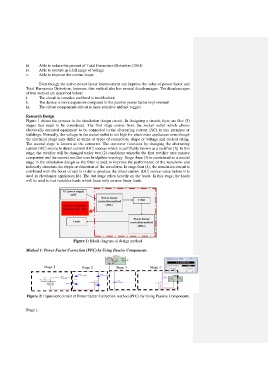
Research Design
Figure 1 shows the process in the simulation design circuit. In designing a circuit, there are five (5)
stages that need to be considered. The first stage comes from the socket outlet which allows
electrically operated equipment to be connected to the alternating current (AC) in any premises or
buildings. Normally, the voltage in the socket outlet is too high for electronics appliances even though
the electrical plugs may differ in terms of types of connectors, shape or voltage and current rating.
The second stage is known as the converter. The converter functions by changing the alternating
current (AC) source to direct current (DC) sources which is certifiably known as a rectifier [7]. In this
stage, the rectifier will be changed under two (2) conditions whereby the first rectifier uses passive
component and the second rectifier uses bridgeless topology. Stage three (3) is considered as a crucial
stage in the simulation design as the filter is used to improve the performance of the waveform and
indirectly eliminate the ripple or distortion of the waveform. In stage four (4), the simulation circuit is
combined with the boost circuit in order to produce the direct current (DC) source value before it is
used in electronics appliances [8]. The last stage relies heavily on the loads. In this stage, the loads
will be used to test variables loads which focus only on non-linear loads.
Figure 1: Block diagram of design method
Method 1: Power Factor Correction (PFC) by Using Passive Components
Stage 1 Stage 2 Stage 3 Stage 4
Figure 2: Equivalent circuit of Power factor Correction method (PFC) by Using Passive Components
Stage 1: